


Abstract
An all-digital beamforming radar system is dependent on the degree to which the transmit and receive channels are synchronized. Since the phases to all channels are applied in the digital domain, there arises a need to establish a known phase and repeatable difference between all the channels. This article discusses a methodology to synchronize multiple modular circuit boards, equipped with high speed data converters, to build a concept of a scalable digital beamforming system. This work involves achieving phase repeatability over power cycles by syncing multiple mixed-signal front-end (MxFE®) integrated circuits (ICs), a four-transmit and four-receive data converter with high on-chip digital signal processing (DSP) capability.
Introduction
Part 2 of this series focuses on implementing the concepts described in Part 1 through both software and hardware to achieve phase repeatability over power cycles.
Experimental Setup with the Digitizer and FPGA Boards
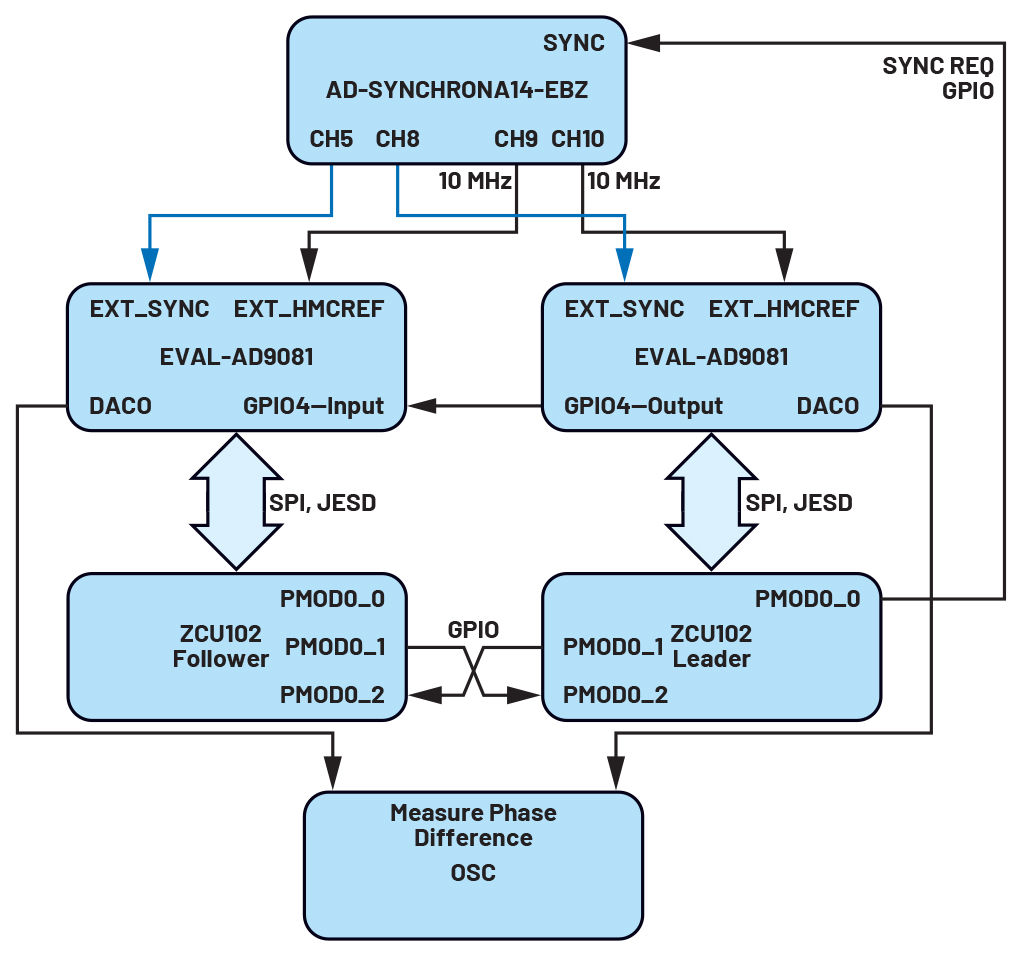
Figure 1 presents the experimental setup used to implement leader-follower synchronization of the two AD9081-based systems. It consists of two EVAL-AD9081 evaluation boards, two ZCU102 MPSoC evaluation kits1, one AD-SYNCHRONA14-EBZ multichannel system clocking device, and an oscilloscope. The connections between the components are also presented in the figure.
The AD9081-FMCA-EBZ evaluation board includes all of the support circuitry required to operate the AD9081 in various modes and configurations, allowing the selection of an external reference clock and synchronization signal for the HMC7044-based clocking subsystem. This was achieved by modifying a switch on both mixed-signal front-end (MxFE®) evaluation boards (R1E resistor unmounted and R2E resistor mounted). The ZCU102 evaluation kit implements the control of the AD9081 devices based on the no-OS framework and the default AD9081 project, as the following subsection will show. The project was modified to implement leader-follower multichip synchronization (MCS). The AD-SYNCHRONA14-EBZ multichannel system clocking device can generate highly accurate frequency and phase-controlled source clocks satisfying the requirements of the implemented MCS method. In the presented setup, it provides the external 10 MHz reference clocks for both the HMC7044 chips on the two AD9081 evaluation boards and generates the pulse required for their synchronization. The oscilloscope is used to test the correct operation of the system and for debugging purposes. Synchronization is considered correct if the phase difference between resets or power cycles remains at the same value.
Firmware and Software Application
Open-source repositories provided by Analog Devices were used to write the code and generate the FPGA image with which the ZCU102 platforms were programmed. Both the no-OS and hardware description language (HDL) sample projects targeting the AD9081 were modified to implement the actions required for synchronization (no-OS sample project, HDL project).
FPGA Image: A modified version of the default HDL AD9081 project was required, one that exposes PMOD0 0, PMOD0 1, and PMOD0 2 pins on the ZCU102 board. The signal on the PMOD0 0 pin of the leader ZCU102, programmed as an output, requests the synchronization signal from the AD-SYNCHRONA14-EBZ clocking device, while the next two general-purpose input/outputs (GPIOs), set up as out-put and input, respectively, are used to ensure that the two AD9081 ICs’ actions align correctly when the numerically controlled oscillator (NCO) synchronization action is triggered.
no-OS Code: A bare metal approach was used to program the ZCU102 systems. The development branch presents modifications of the AD9081 no-OS sample project. Modifications to the HMC7044 and AD9081 drivers and to the AD9081 project were performed as follows.
- HMC7044 driver: make the program wait until the HMC7044 receives a SYNC pulse when set in external sync mode.
- AD9081 driver: implement leader-follower logic, add synchronization GPIOs for ensuring that all AD9081s in the system wait for the synchronization pulse at the same moment in time, add the possibility of running the NCO test; the synchronization source of the AD9081 is set to SYSREF, so that the internal clocks are aligned with this signal.
Appropriate settings were required in the sample project so that the correct way of working is selected. These modifications are performed for both the leader and the follower.
- EXT HMCREF is set as the preferred reference clock for the HMC7044.
- External synchronization input is enabled for the HMC7044.
- Selection of continuous SYSREF signal.
- The addition of two GPIOs to ensure that the programs running on the two ZCU102 systems reach the AD9081 synchronization at the same time.
The no-OS code uses the finite state machine (FSM) JESD to bring up the JESD links to transfer ADC/DAC data. A new device was added to the JESD topology: a GPIO that is controlled by the leader and that requires the synchronization pulse for the two HMC7044s on the AD9081 development boards, during the clock synchronization stage. All modifications in the no-OS projects are listed on the ADI no-OS webpage.
AD-SYNCHRONA14-EBZ Settings: The default device tree overlay of the AD-SYNCHRONA14-EBZ was modified to provide the 10 MHz clock outputs (enclosure Channel 9 and Channel 10) used as external references by the HMC7044 chips on the AD9081 evaluation boards and the pulse used for their synchronization (enclosure Channel 5 and Channel 8). These channels belong to the HMC7044 FPGA mezzanine card (FMC) node in the device tree overlay, corresponding to the top HMC7044 in our setup. The settings are chosen in such a way that the SYNCHRONA system generates aligned signals and that the pulse that is requested via the SYNC input is synchronized with the 10 MHz outputs.
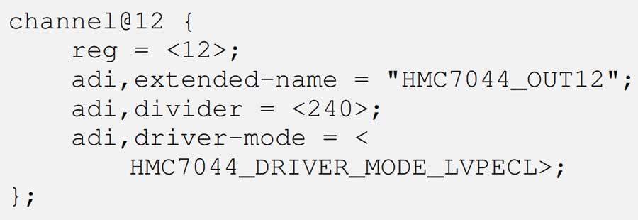
The settings of a 10 MHz reference clock channel are listed in Figure 2. The same settings apply to both HMC7044 channels, 5 and 12.
The general settings of the HMC7044 that outputs the 10 MHz reference clocks and the sync signals are presented in Figure 4. Pulse generator mode is set to one pulse, so that the AD-SYNCHRONA14-EBZ system outputs a single impulse synchronized with the 10 MHz output when it receives a command via the SYNC input.
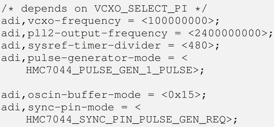
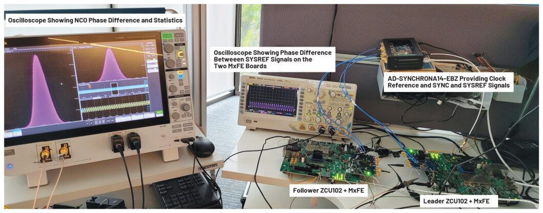
Figure 5 shows the experimental setup built for the synchronization of the NCO signal on both AD9081 development boards. An additional oscilloscope is present here in the center of the figure, being used for debugging during development, and it shows the aligned SYSREF signals from the two HMC7044 ICs on the two MxFE evaluation boards. The oscilloscope on the left of Figure 5 shows the phase difference of the NCO and the statistical values as histograms of the difference in degrees and picoseconds between the signals on the two channels.
The overall implemented procedure is as follows:
- Configure the HMC7044 on the EVAL-AD9081 to assign the highest priority to the 10 MHz clock that enters the boards from the AD-SYNCHRONA14 module. The HMC7044 can accept multiple reference inputs and will select the appropriate source based on the priority control set by the user.
- Configure the HMC7044 on the EVAL-AD9081 for external synchronization. Modify the driver so that the device waits until the external sync signal has been applied.
- Add an MCS GPIO as a device in the JESD FSM topology, which triggers the synchronization of the two HMC7044 ICs by sending a request to the AD-SYNCHRONA14. The follower will have to be powered/restarted first of the two ZCU102 + AD9081 systems, and will wait for the SYNC pulse. The leader will request the pulse through a connection between PMOD0 0 of the leader ZCU102 and the SYNC input of the AD-SYNCHRONA14. Only the leader has a physical connection between the MCS GPIO (PMOD0 0) and SYNC on the AD-SYNCHRONA14.
- The leader will advance in the program and wait before triggering the NCO reset until it reads 1 on the PMOD0 2 input, signaling that the follower is ready.
- The follower will set the output pin (PMOD0 1) to 1 after setting the synchronization parameters. This pin is connected to the input (PMOD0 2) of the leader ZCU102, waiting (see previous step). At this point, the follower is ready to synchronize and waits for the command on the selected GPIO (GPIO 4 in Figure 1, which is a GPIO pin on the AD9081 evaluation board). After this point, it will wait until the value on the input pin (PMOD0 2) is 1.
- The leader will see that the input pin state is now 1 and will advance in the program, triggering multichip synchronization. Afterwards, it will also change the output pin value (PMOD0 1) to 1 so that the follower can acknowledge it and advance in the FSM also.
- The phase difference measured between DAC0 of both AD9081 ICs will have the same value over resets/power cycles.
- Once this phase difference has been measured, the appropriate NCO phase application programming interface (API) could be called after the ad9081_init function to compensate for this phase offset and in this way have aligned waveforms from both AD9081 evaluation boards. One board could be used as the reference, and the phase offset shall be applied to the other boards’ channels.
Results and Conclusion
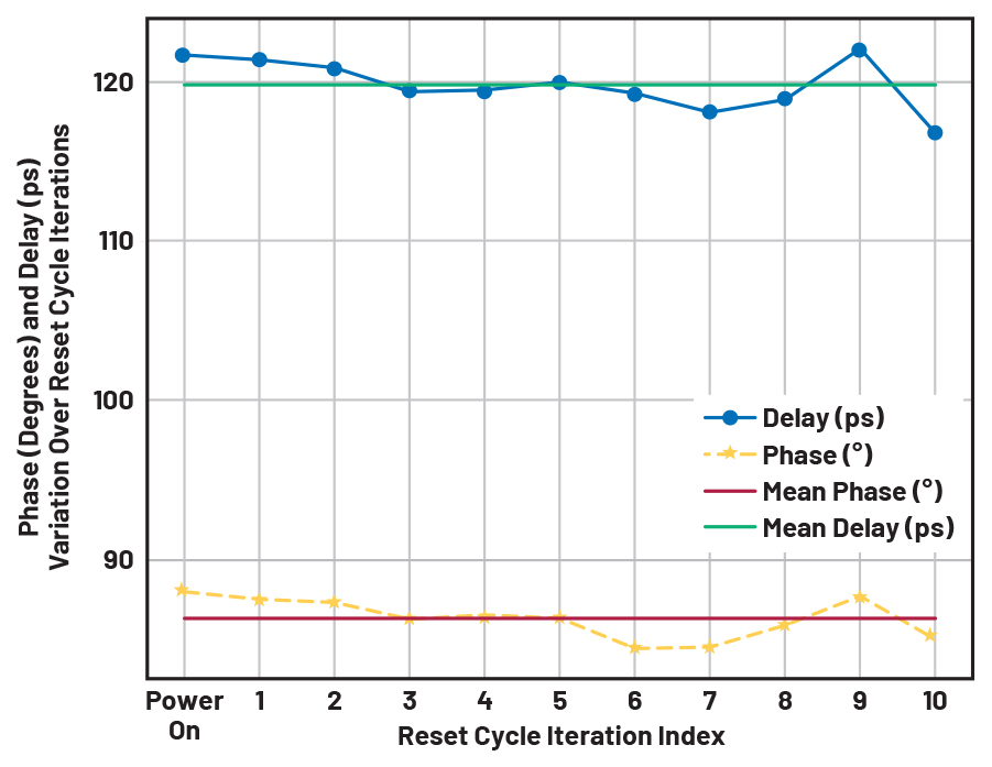
Figure 6 shows the phase difference in degrees and picoseconds and the corresponding histograms generated over a period of several minutes. Table 1 shows the phase data over multiple power cycles between the two DAC outputs of the AD9081s from different boards.
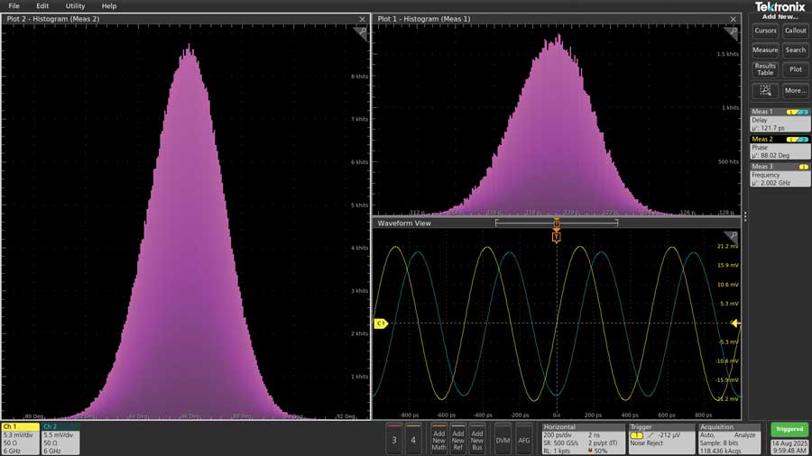
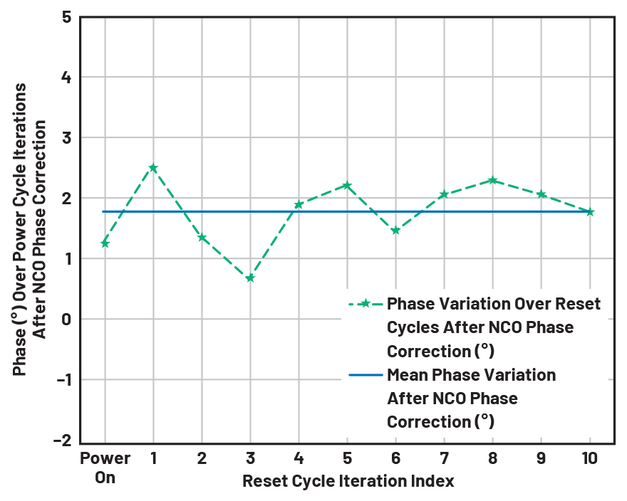
The results show the repeatability of the output phase from the two boards’ DAC outputs. Based on the mean of the statistics, it is evident that the phase (time delay at 2 GHz) is indeed repeatable with fair accuracy. The work intends to continue gathering more data over power cycles to have a good statistical representation of the repeatability. The mean of the phase difference is 86° and the mean of the time difference is 119.8 ps. The phase difference between the reset cycles is presented in Figure 7.
Table 1. Delay and Phase Difference After Resets
| Reset No. | After Power On | 1 | 2 | 3 | 4 | 5 | 6 | 7 | 8 | 9 | 10 |
| Delay (ps) | 121.7 | 121.4 | 120.9 | 119.4 | 119.5 | 120 | 119.3 | 118.1 | 118.9 | 122.1 | 116.8 |
| Phase (°) | 88.02 | 87.55 | 87.35 | 86.3 | 86.57 | 86.36 | 84.46 | 84.55 | 85.92 | 87.75 | 85.03 |
| Phase After NCO Correction (°) | 1.3 | 2.55 | 1.41 | 0.7 | 1.92 | 2.24 | 1.48 | 2.08 | 2.32 | 2.09 | 1.81 |
Once the phase differences between the channels of both boards have been determined, the phases can be corrected through the phase control of the NCOs. The functionality has been exposed through the APIs in the firmware. As discussed in Part 1, these phase values could be stored in a lookup table (LUT). The last row in Table 1 shows the phase difference over reset cycles after the follower phase, the yellow signal in Figure 6, has been compensated for a difference of –86° (Figure 8).
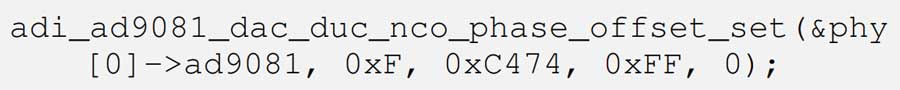
The AD9081 allows an asynchronous update of the NCO phases, and hence this could be applied after the top level initialization API has run completely. The API for NCO phase correction has been used to compensate for the repeatable phase difference, and the mean difference after this correction is 1.8° from the data in Table 1, presented graphically in Figure 9.
In the future, we would also like to evaluate the influence of temperature variation across the boards on the phase stability over time. The HMC7044 has a phase-locked loop (PLL) that locks to a low frequency clock fed externally and is susceptible to phase shifts due to temperature gradients on both boards. This phase shift in the clock would manifest itself as a phase shift in the output of both boards that would change as the temperature gradient changes on both of them, and hence we expect a drift in the phase difference from both boards. The concept and dependence of phase on temperatures in PLLs has been described in “Power-Up Phase Determinism Using Multichip Synchronization Features in Integrated Wideband DACs and ADCs.” This work, specifically, demonstrates a method for achieving synchronization between two PLL + clock distribution ICs (HMC7044) and then builds on it to demonstrate phase repeatability through the MxFE family of devices.
Reference
1UG-1182: ZCU102 Evaluation Board User Guide. Advanced Micro Devices, Inc., February 2023.


