

PICs (photonic integrated circuits) make it possible for optical communication to take place not only using fiber optics and separate parts but also in the semiconductor environment. This means that PIC technology combines all separate parts into one single chip and enables information to travel as light that is generated by laser instead of being transmitted with electric signals.
This matters because the amount of data transfer conducted with the help of AI systems is growing significantly. Recent examples of successful projects involved the use of 3D photonic systems with light transmission rates of 800 Gb/s.
The Role of Photonics in Electronics
Electrical interconnects are effective over a short distance, but as bandwidth increases, so do the losses and the power consumption. Copper interconnects also encounter a certain number of limitations, such as the signal attenuation, the resistive component of current, and the heating. Photonics eliminates these disadvantages by enabling the use of many optical channels and wavelength-division multiplexing.
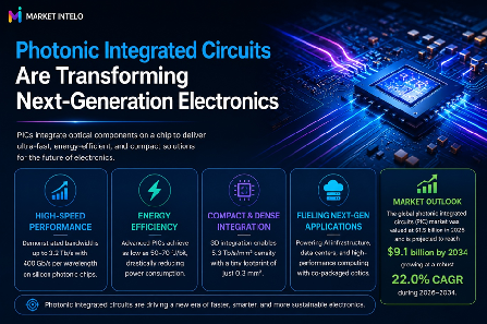
The prospects of growth speak in favor of the role of this technology. Market Intelo reports that the world’s market of photonic integrated circuits had around $1.5 billion in 2025 and will grow up to about $9.1 billion in 2034, which means CAGR of 22.0%. The growth is connected to the increasing demand for high-speed optical connectivity.
Hence, one optical path can transmit multiple data streams thus the recent findings achieved a total transmission capacity of 3.2 Tb/s on a chip with the ability of transmission using 8 channels including 400 Gb/s on each channel.
Functionality of Photonic Integrated Circuits (PICs)
A PIC operates by receiving electrical signals, transforming them into light signals, directing the light through waveguides, and subsequently converting them back to electrical signals through a photodetector. Silicon is the commonly used material due to its ability to be processed using dominant CMOS-compatible processes and for producing wafers of a large diameter.
However, the use of different materials, including indium phosphide, silicon nitride, and lithium niobate, allow creating what is missing in silicon – light generation or low-loss modulation technologies.
Latest implemented developments in optical technology enabled packing more than 80 optical transmitters and receivers on 0.3 mm². Thus, the system produced a speed of 800 Gb/s with the single channel of 10 Gb/s, demonstrating that a lot of low-speed channels may be combined into a single high-speed channel.
Major Areas of Development
The development of PIC is currently focused on techniques that can produce devices that will offer better bandwidth performance, as well as exhibit lower power consumption, compact size, and ease of production.
- Modulators developed in silicon, released in 2025, achieved electro-optical bandwidths of up to 110 gigahertz and transmission speeds of 110 and 130 gigabits per second.
- Dense integration: the use of 3D technology has achieved channel density of 5.3 terabits/s/mm², obtaining a power consumption of only 120 fJ/bit of data transmitted.
- Packaging: a fan-out wafer-level silicon photonic engine has obtained a transmission rate of 1.79 terabits per second, using 8 channels at 224 Gb/s.
- Wavelength scaling: Achieved in a recent study involving 8-channel technologies. The performance of achieved technologies is around 3.2 Tb/s, with the transmission capacity of 400 Gb/s for one channel.
It can be concluded that the progress happens at the device, chip, and packaging levels simultaneously.
Recent PIC Developments at a Glance
| Development Area | Reported Numeric Value | Significance |
| 3D photonic interconnect | 800 Gb/s | Supports high-density chip-to-chip communication |
| Photonic channel count | 80 channels | Increases aggregate bandwidth through parallel data transfer |
| Channel density | 5.3 Tb/s/mm² | Demonstrates compact optical integration |
| Wavelength-based transmission | 3.2 Tb/s total | Shows the potential of multi-channel optical communication |
| Per-wavelength capacity | 400 Gb/s | Increases bandwidth without adding separate physical links |
| Fan-out photonic packaging | 1.79 Tb/s | Advances high-bandwidth optical packaging |
Recent Trends in Research and AI Technology
A significant advancement in technology is the application of photonics to enhance communications in the AI setup. In one such breakthrough, scientists demonstrated an integration of electronics and photonics in a 2025 study appearing in Nature Photonics, achieving the communication rate of 800 Gb/s across 80 channels.
At the same time, the transmitter and receiver units required 50 fJ and 70 fJ of energy per transmitted bit at 10Gb/s respectively. The area occupied by photonics was 0.3 mm² while the density measured 5.3 Tb/s/mm². As a result, photonics integrated circuits reduce length of the electrical paths and boost the bandwidth capacity by moving the optical conversion process nearer to the processors.
The Rise of Co-Packaged Optics in Data Centers
Co-packaged optics refers to the technology of co-packaging photonic integrated circuits (PICs) and electronics chips (ECs). Instead of placing optical transceivers far from the processor and needing to electrically connect components, CPO allows the optical engine to be integrated into the chip with the switching transistor.
Research has shown that the technology has already produced optical engines operating at speeds of 1.6 Tb/s. Other studies have achieved speeds of 1.79 Tb/s with an additional eight lanes of chips used. Roadmaps in the optical communications do not stop at 800 G and 1.6 T speeds.
Engineering Challenges Ahead
Manufacturers of photonic integrated circuits encounter difficulties in manufacturing and system integration. Factors like optical alignment, thermal stabilization, laser integration, packaging yield, and material compatibility can impede the production of PICs. Even temperature shifts of a few Celsius degrees can alter the properties of resonant optical devices and require tuning for proper operation.
Manufacturing also requires a precision level that dictates the use of waveguide structures with dimensions in the order of hundreds of nano meters.
Development for the Future
The development of photonic integrated circuits has established them as a bridge between electronics and optical communication. The latest achievements indicate the ability of these circuits to use chip-level capacity of up to 3.2 Tb/s, create dense links at a speed of 800 Gb/s, and deliver up to 400 Gb/s per wavelength with tens of femtojoules of energy expenditure per bit.
The next stage will determine the integration of lasers, photonics, electronics, and thermal management into packages suitable for mass production. As the requirement of AI, data centers, sensing, and communication increases, it can be expected that PICs will be used to work with light in the future electronic systems.