

At its recent Global Imaging Media Briefing, STMicroelectronics presented its vision for the future of imaging, demonstrating how image sensors are evolving from conventional cameras into intelligent sensing platforms that power the next generation of Edge AI systems. During the briefing, ST introduced two key additions to its imaging portfolio: a new compact direct Time-of-Flight (dToF) 3D LiDAR module for Edge AI systems and a new series of 5-megapixel CMOS image sensors designed to accelerate and simplify innovation.
With applications spanning robotics, industrial automation, automotive safety, smart buildings, wearables and IoT, ST aims to accelerate the adoption of intelligent vision systems that process data closer to the edge while preserving privacy and reducing system complexity.
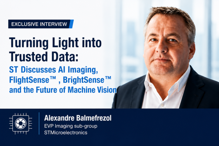
In this interview with Pratibha Rawat from Electronics Media, STMicroelectronics, Alexandre Balmefrezol , EVP Imaging sub-group, discusses the company’s imaging strategy, its differentiated approach to machine vision, and how intelligent sensors are transforming the future of AI-powered devices.
Q1. Image sensors have traditionally focused on capturing pictures. How is artificial intelligence changing the role of imaging sensors?
Artificial intelligence is fundamentally transforming the purpose of imaging sensors. In the past, sensors were designed mainly to capture high-quality images for human viewing. Today, their role extends far beyond photography. Modern sensors are expected to provide meaningful information that allows machines to understand their environment and make decisions in real time.
At ST, imaging sensors are evolving into intelligent sensing devices capable of depth sensing, human presence detection, biometric authentication, context awareness and even perception beyond human vision. Rather than simply producing images, they generate reliable data that AI algorithms can process locally to improve safety, efficiency and automation. This shift enables applications such as autonomous robots, industrial inspection, smart buildings and automotive safety systems, where sensors become an integral part of the AI decision-making process.
Q2. What is ST’s overall strategy in the imaging sensor market, and how does it differ from other sensor manufacturers?
ST has deliberately chosen not to compete in the highly commoditized market for conventional RGB image sensors. Instead, the company focuses on specialized sensing technologies where it can provide greater system-level value.
Its strategy revolves around three major product families: FlightSense for Time-of-Flight (ToF) depth sensing, BrightSense for computer vision applications, and SafeSense for automotive safety solutions. These products are designed to solve specific customer challenges rather than simply offering higher image resolution.
A major differentiator is ST’s Integrated Device Manufacturer (IDM) model. The company controls every stage of development—from pixel design and CMOS process technology to packaging, optics and system integration. Combined with STM32 microcontrollers and software support, ST delivers complete sensing solutions rather than standalone image sensors, enabling customers to accelerate product development with lower integration complexity
Q3. ST recently introduced the VL53L9 FlightSense module. What makes this product a significant advancement in Time-of-Flight technology?
The VL53L9 represents a major step forward because it is ST’s first fully integrated all-in-one Time-of-Flight module. Traditionally, LiDAR systems require customers to integrate multiple components such as laser emitters, optics, sensors, calibration and signal processing. ST has consolidated all of these functions into a single compact module.
The device incorporates the SPAD sensor, laser source, optics, on-chip processing, power management and factory calibration, allowing customers to integrate it much more easily into their products. This greatly reduces engineering complexity while maintaining high measurement accuracy.
The module delivers a ranging distance of up to nine metres indoors, operates at up to 100 frames per second, supports 54 × 42 sensing zones and provides one-degree angular resolution. It is capable of detecting objects from as close as five centimetres while simultaneously monitoring people and objects several metres away, making it suitable for a wide range of AI-based applications.
Q4. Privacy has become an important concern in AI systems. How does FlightSense address this challenge?
Privacy is one of the key advantages of Time-of-Flight sensing compared with conventional cameras. Unlike RGB cameras that capture identifiable facial details, FlightSense produces low-resolution depth information that focuses on object shape and distance rather than personal identity.
This enables applications such as occupancy detection, people counting, fall detection and posture recognition without recording recognizable images of individuals. As a result, organizations can deploy intelligent monitoring systems in offices, healthcare facilities, industrial environments and smart buildings while maintaining user privacy and complying with increasingly stringent data protection requirements.
Q5. ST demonstrated advanced AI processing on an STM32H5 microcontroller. Why is this achievement important?
One of the most impressive demonstrations during the briefing showed sophisticated AI algorithms running directly on an STM32H5 microcontroller without requiring a dedicated AI accelerator.
Using data generated by the FlightSense module, the system could detect human presence, identify falls, recognize body posture, distinguish between sitting and walking, and count multiple people simultaneously. These AI functions operated at 30 frames per second while consuming only a relatively small percentage of the available memory and flash.
This demonstrates that complex AI workloads can increasingly move to low-power edge devices instead of relying on cloud computing or expensive processors. For developers, this means lower power consumption, reduced latency, improved privacy and lower overall system cost.
Q6. BrightSense is positioned as a camera sensor for machines rather than humans. What does that mean in practice?
Traditional camera sensors are optimized to produce visually attractive photographs for people. BrightSense, however, is designed specifically for machine perception, where image quality is only one part of the overall objective.
Instead of maximizing megapixels, BrightSense emphasizes large pixels, high sensitivity, low noise, low latency and efficient power consumption. The sensors are optimized to deliver exactly the information required by AI algorithms while minimizing unnecessary data processing.
This approach enables faster computer vision processing in battery-powered devices such as industrial sensors, robots, wearable products, smart city infrastructure and IoT equipment, where efficiency is often more important than producing visually perfect images.
Q7. What are the key innovations in ST’s new 5-megapixel BrightSense sensor?
The new five-megapixel BrightSense sensor combines several advanced imaging capabilities within a single device. It features large 2.25-micron pixels that improve image sensitivity while maintaining low noise performance.
One of its most significant innovations is hybrid shutter technology, allowing the same sensor to operate in both rolling shutter and global shutter modes. Rolling shutter provides excellent image quality for conventional imaging, while global shutter eliminates motion distortion when capturing fast-moving objects.
The sensor also supports RGB, monochrome and Near-Infrared imaging, making it suitable for applications ranging from industrial automation and robotics to smart city surveillance and AI-based machine vision.
Q8. ST frequently highlights its meta-surface optics and 3D stacking technologies. Why are these technologies important?
These technologies play a critical role in improving sensor performance while reducing system size.
Meta-surface optics allow ST to precisely shape and control light using extremely thin optical structures, enabling smaller, lighter and more efficient optical modules compared with traditional lenses. At the same time, 3D stacking separates the imaging pixels from the processing circuitry, allowing each layer to be independently optimized.
This architecture improves sensitivity, increases quantum efficiency, reduces module size and enables the integration of advanced image processing functions directly within the sensor. Together, these innovations help deliver higher performance while maintaining the compact form factors required by modern AI devices.
Q9. Where does ST see the biggest opportunities for its AI imaging technologies?
ST sees significant growth opportunities wherever machines require reliable visual perception while operating with limited power and computing resources.
Target applications include industrial robotics, warehouse automation, smart buildings, healthcare equipment, autonomous mobile robots, AR/VR devices, smart farming, gaming, humanoid robots and advanced automotive systems.
The company believes that combining depth sensing with computer vision will enable machines to better understand their surroundings, improving safety, efficiency and automation across a broad range of industries.
Q10. Looking ahead, how will AI reshape the architecture of future vision sensors?
According to ST, future vision sensors will become increasingly intelligent rather than simply serving as image capture devices. Instead of transmitting large volumes of raw image data to external processors, sensors will perform much of the data processing locally.
This requires a new sensor architecture focused on lower resolution, lower power consumption, embedded AI processing and reduced data transfer. Features such as event detection, object recognition and scene analysis will increasingly be integrated directly within the sensor itself.
As AI continues moving toward the edge, imaging sensors will evolve into intelligent perception systems capable of delivering only the most relevant information to the host processor. This approach reduces latency, improves energy efficiency, enhances privacy and enables a new generation of autonomous and connected devices.