Situation:
A market-leading enterprise switch manufacturer needed to migrate from GbE to 10GbE on an enterprise switch design.
Solution:
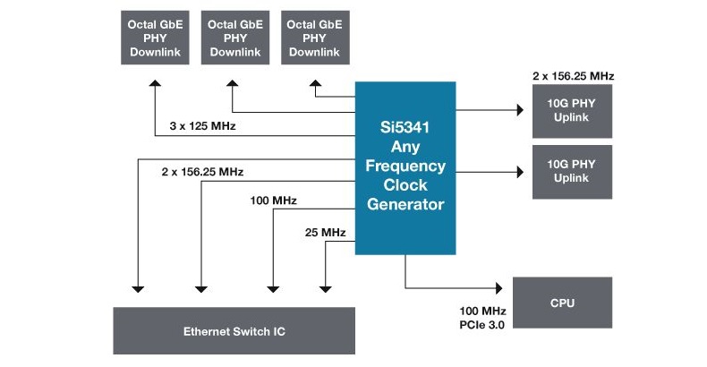
Since 10GbE has more stringent jitter requirements than GbE, the customer designed in the ultra-low jitter Si5341 clock generator. This single device provides all PHY, switch and CPU clocks, simplifying design while providing 80% margin to system-level jitter specifications.

Benefit:
Silicon Labs’ patented technology enables a single clock generator to synthesize any combination of clocks, enabling a single-chip clock tree for most applications. Industry-leading jitter performance of 100 fs RMS helps ensure first pass design success and minimized error rates in high-speed data communication systems.

Timing Fundamentals:
- Clock Tree: The combination of devices, including clock generators, oscillators and buffers that generate, distribute and synchronize the clock signal(s) in a system
- Jitter: Timing variation of a clock signal from its ideal value
- Jitter Margin (aka jitter budget): Jitter margin is the difference between the actual system jitter and the allowable jitter which still supports a given data rate
For more information visit: www.silabs.com


