


Implementing run-time fault detection for SRAM (Static Random-Access Memories) using checkerboard algorithms presents practical challenges
In the design of safety critical systems, there are several international safety standards that help guide safety engineers to select appropriate processes and techniques to minimize critical faults in the end product. While these standards play a significant role to make sure that past oversights are not repeated, it is important that safety engineers have sufficient knowledge of the underlying hardware, such as a microcontroller, to ensure that the standards are implemented correctly. Otherwise, there is a potential danger that less experienced safety engineers may implement unsafe designs. For instance, the IEC (International Electrotechnical Commission) 60730 standard recommends the use of a checkerboard memory test to identify DC faults in variable memories for Class B software. While this may seem straightforward at first glance, it may be more challenging than expected.
For instance, the logical and physical layouts of the SRAM on a microcontroller can have several undocumented differences. Without the knowledge of these differences, one may inadvertently implement memory tests such as the checkerboard algorithm without the correct diagnostic coverage. While the required information may not be available in the datasheet of standard microcontrollers, the challenge can be addressed by using memory test algorithms that are not influenced by the differences between the logical and physical layouts of the SRAM.
Testing SRAM for Run-time Defects
All SRAM memories are tested by vendors during production and defective products are not shipped to consumers. Despite this, random hardware defects will likely appear during the lifetime of the integrated circuit (IC). For this reason, any safety critical application must include diagnostic tests of the hardware, such as the SRAM, at run-time.
The Checkerboard Memory Test
As per safety standards such as the IEC 60730 (H.2.19.6.1), a checkerboard algorithm can help identify certain defects (DC faults) in SRAM for applications required to comply with the Class B safety level. The checkerboard test is generally used as it covers the most common faults in an SRAM. In addition, the algorithm can be executed comparatively fast, making it convenient to minimize the performance impact on the application itself. Not only does this help detect DC faults where a bit is permanently stuck high or low, the checkerboard algorithm is also capable of identifying defects where neighboring bits affect each other.
Logically, an SRAM consists of several bits organized in words that are typically 8-, 16- or 32-bit wide, or even longer. In a physical SRAM, the bits are organized in arrays as shown in Figure 1. Each bit typically has eight neighboring bits. When a physical defect occurs in a bit, it can either affect a single bit to be stuck high or low (DC fault), or the defect can be in the separation of two bits. In this case, a neighboring aggressor cell (marked in purple in Figure 1) may influence a victim cell (marked in yellow in Figure 1). The aggressor-victim scenario is known as a coupling fault. While the DC fault is more prevalent statistically, it is also important to detect the most likely coupling faults.
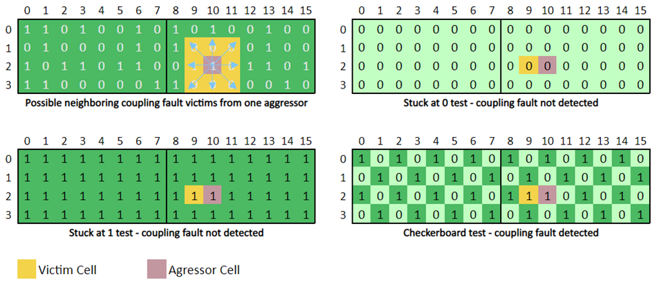
In the event that a fault is affecting a single bit, such that the bit is stuck high or low, the error can be revealed by writing the value one and verifying the one by reading it back, and next writing the value zero and verifying the zero by reading it back as illustrated in Figure 1. Alternatively, if the defect is due to a coupling fault between two neighboring bits, say bit columns 9 and 10 in row 2, writing certain patterns, such as all ones or all zeros does not reveal the coupling fault as the cells have the same value during the test.
Coupling faults also occur where the neighboring cells (to the sides, above, and below) have opposite binary values. As Figure 1 (lower right) illustrates, the logical one in bit 10 has contaminated bit 9, and the coupling fault is revealed since bit 9 does not hold the expected value, zero.
Differences between Physical and Logical Layouts of SRAM
Datasheets usually only describe the logical layout of the SRAM and not how the SRAM is physically organized. This makes it challenging to correctly implement the checkerboard algorithm since it requires knowledge of neighboring bits.
One way to understand the physical layout of the SRAM is to make the distinction between bit-oriented memories (BOM), where one bit can be accessed at a time, and word-oriented memories (WOM) in which an n-bit word is read and written at a time. Despite most real-world memories being implemented as WOM, the classic memory testing algorithms in scientific literature often assume BOM implementations.
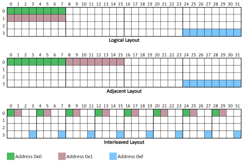
In the case of WOM memories, bits can be physically organized according to three main categories: adjacent, interleaved, and sub-arrays. While each word is placed below the previous word in the same column (address space-like) in a logical layout, adjacent memories place each word in the same row next to each other as shown in Figure 2. For interleaved architectures, each bit of the word is separated into different columns and rows of the SRAM array. In sub-array organization, each bit of a word is placed in different physically separate blocks of the SRAM. The issue is that a safety engineer will normally not have access to this information regarding the physical layout, which is required to implement a checkerboard test properly.
Properties and Shortcomings of the Checkerboard Algorithm
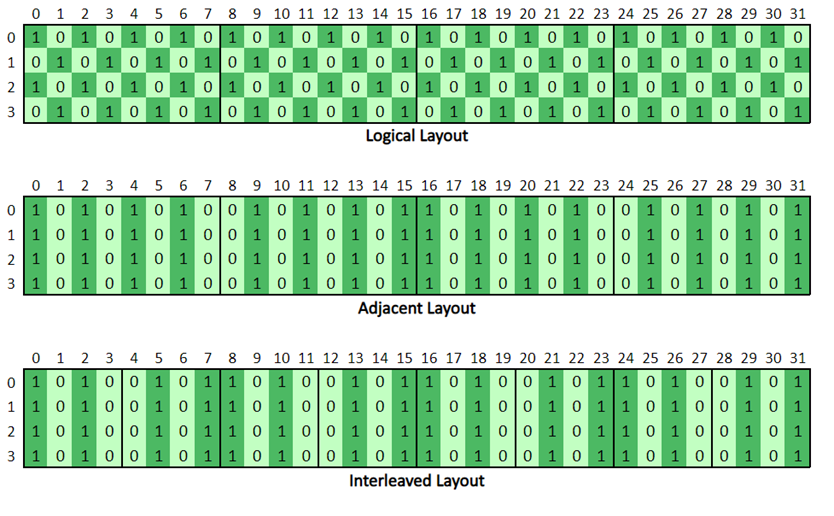
When it comes to implementing a checkerboard algorithm, one approach that seems reasonably straightforward is to simply write the value 0xAA (assuming 8-bit data words) to the first address and 0x55 in the next address alternately. This is repeated until all addresses under testing have been filled with the checkerboard pattern of ones and zeros. After verifying the pattern to detect any DC or coupling faults between neighboring cells, the process is duplicated using the inverse pattern. While this seems simple enough, there is a catch. As mentioned earlier, there can be differences between the logical and physical layouts. So, the checkerboard pattern in the logical layout of the memory may not be the same as the checkerboard pattern in the underlying physical layout as shown in Figure 3.
It is difficult to compensate for the differences between the logical and physical layouts since the necessary information is usually unavailable in the datasheet of the device. That leaves us with a few options. First, accepting the lower coverage, especially since the diagnostic still covers DC faults and some coupling faults between neighboring bits. The second option is to request the layout from the IC vendor and make a custom implementation of the checkerboard test for each device. Lastly, one may choose to select a different algorithm instead.
With this awareness of the potential shortcomings of the algorithm, safety engineers can make a more informed decision when selecting their run-time memory testing approach.
Alternatives for Run-time Testing of SRAM
IEC 60730 proposes certain memory testing techniques for the Class C safety level with higher fault detection coverage. These techniques fall into the category of production test algorithms. While they take a longer time to run, they can detect less common fault types. However, since they operate on the entire SRAM and not in sub-blocks, they typically destroy the data stored in the SRAM. As this is not ideal for our embedded designs, we propose hybrid March algorithms adapted from the production test March algorithm. These algorithms are available in WOM-optimized implementations and offer high test coverage. These hybrid March algorithms can be implemented such that they run on smaller overlapping sections of the SRAM. This approach can ensure that no SRAM data is lost during testing, thereby eliminating the need for a reboot of the embedded system. One drawback of the March algorithms is that they are computationally heavier compared to traditional checkerboard algorithms. However, depending on the requirements of the safety application, this might be an unavoidable expense.
Some microcontroller vendors offer the option to swap a traditional checkerboard test with a March test. Microchip, for instance, as part of its software diagnostic libraries, offers performance-optimized implementation of a March C- algorithm. The Microchip implementation supports testing of the entire SRAM, which is normally done at start-up to get maximum test coverage. It also supports the testing of smaller, overlapping memory blocks, in order to reduce the real-time impact on the application. The implementation can be downloaded for free from Microchip’s website as part of the IEC 60730 Class B library. The implementation is for PIC and AVR microcontrollers but can also be ported to other Microchip MCUs.
For more information about IEC 60730 Class B tests: https://www.microchip.com/PIC-AVR-IEC60730


