


High Density Interconnect PCB
Technology is evolving day by day with a fast pace of advancement in each and every sector. It is bringing new innovative designs and products that not only provide the best in the industry but also minimize the cost while saving space. Over the last couple of decades, the need of packing more capabilities into smallest packages or miniaturization of devices has come into play. Today the Tech Design Engineers and Component Manufacturers are working on the spaces saving and cost effective techniques to make the miniaturized form of electronic devices so as more components are packed on a single board in a smaller space as possible.
This miniaturization of hardware is also taking place in Printed Circuit Boards (PCBs) so as to make the electronic devices or components more portable and compact without any compromise in the quality, speed, performance, power consumption, or functionality of the devices. Today, if we talk about the PCB industry, then the HDI Technology is one of the fastest-growing technologies in this sector which is making the electronic devices more convenient. In this article we will discuss about High Density Interconnect PCB Technology , their application areas and why you should choose the HDI PCBs for your designs.

What is High Density Interconnect PCB (HDI PCBs)?
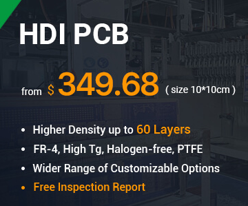
HDI PCB Technology refers to High-Density Interconnect PCB, a printed circuit board having higher wiring density per unit area as compared to conventional PCBs. Designing a printed circuit board using HDI PCBs techniques enable more components to be packed in a smaller space. These PCBs includes high-density attributes like microvias, blind and buried vias, sequential lamination, fine lines and spaces, and via-in-pad techniques along with thin traces that help reduce size, weight and pack more components into a smaller area while enhancing the electrical performance of embedded devices.
To produce a high density circuit board, these High-Density Interconnect PCBs deploy microblind buried hole technology and supports about 4 to 24 number of layers. They consist of high circuit density as compared to traditional circuit boards and leads to BGA pitch reduction, line reduction, space reduction, board thickness reduction, via diameter reduction etc.
Advantages of High-Density Interconnect PCBs
There are numerous advantages of HDI PCBs some of them are:
High-Density Interconnect PCBs are compact, lightweight, more durable and efficient PCBs, brings down the board space requirements.
They can be populated on both sides of the board, thus helps designers to incorporate more components onto smaller boards.
Improves signal integrity due to shorter signal paths, all thanks to its via-in-pad technology that cuts down the signal path lengths.
Offers better durability and reliability in hazardous and extreme environment as its HDI technology makes route and connect easier.
Ideal for battery powered and handheld devices as they decrease power usage, results to longer battery life of the devices.
Offers denser trace routing light weight and small size PCBs with high reliability while enhancing the electrical performance of the device.
Allow for more efficient and fast signal transmission with enhanced signal quality.
They are cost effective and reduce the entire size and weight of final products as numbers of necessary layers are reduced.
They reduce thermal degradation and increase circuit density and design efficiency.
Creating an High Density Interconnect PCB is very less time-consuming as the amount of components need to develop an HDI board are not a lot.
Applications of High Density Interconnect PCB
Due to their compact, cost-effective, lighter in weight and size High Density Interconnect PCBs are ideal for complex small form-factor designs. Some of their application areas are as follows:
- Medical Electronics: Being miniaturized, these PCBs are widely used in the medical industry as they can fit in small medical devices like pacemaker, implants, imaging diagnostic equipment etc.
- Automotive: HDI technology plays an increasingly important role in the automotive industry. Cars are becoming more computerized and connected, the need for many advanced features such as GPS, onboard WiFi, backup sensors, and rear-view cameras are widely used and all of them rely on HDI PCBs.
- Portable & Digital Devices: They are used in smartphones, tablets, touch-screen devices, laptops and other handheld and portable electronic devices.
- Aerospace and Military: As High Density Interconnect PCB offer better durability and reliability in extreme environment and hazardous conditions, therefore they are well suited for defence and aerospace applications.
- Wearable Devices: The wearable technology is gaining tremendous popularity and so as HDI PCBs because miniaturization is the key for the application of these products.
Conclusion:
The Printed Circuit Boards industry plays a very important role in the development of electronic devices. The growing adoption of PCBs in various industries with the demand for excellent performance while conserving space have increased the need of High Density Interconnect PCB. High Density Interconnect PCB technology not only give engineers unprecedented design freedom but also provide flexibility while allowing smaller components to be placed together. Miniaturization is the key to the effective application of the product and here High Density Interconnect PCB Technology plays its role very well in making electronics devices fit anywhere.


