


Abstract
Apollo MxFE Technology – Superconducting quantum computers demand precise, phase-coherent microwave control and low-noise readout—requirements that strain traditional, discrete RF architectures. This article shows how Analog Devices’ Apollo MxFE integrates high-speed RF DACs/ADCs, on-chip digital signal processing, and deterministic synchronization to enable direct-RF qubit control and measurement. Paired with ADI’s clocking and local oscillator solutions, the platform reduces system complexity, power, and latency while improving scalability and gate fidelity, positioning it as a core enabler for next-generation quantum systems.
Introduction to Computing Paradigms
Quantum computing is moving rapidly from research labs into practical systems with the potential to reshape drug discovery, materials design, optimization, climate modeling, and cybersecurity. By exploiting quantum-mechanical effects such as superposition and entanglement, quantum processors can address problem classes that overwhelm classical architectures—including cryptographic schemes built on today’s public-key encryption. Among competing hardware approaches, superconducting transmon qubits have emerged as a leading platform thanks to their maturity, scalability, and compatibility with microwave control.1 These devices rely on precisely shaped RF pulses in the 4GHz to 4.5GHz range, placing stringent demands on the underlying electronics. This article introduces a cost-effective, high-performance RF pulse-generation architecture built on ADI’s AD9084 Apollo MxFE platform, designed to deliver the precision, speed, and scalability required for next-generation quantum systems and progress toward fault-tolerant computing.
Quantum Computing System Platform Architecture
Quantum Information, Superposition, and Pulse-Based Control
The most recognizable image of a quantum computer is a golden chandelier suspended from a dilution refrigerator. However, the underlying technology spans multiple approaches and/ or techniques, including superconducting circuits, photonic qubits, silicon spin qubits, and trapped ions. Regardless of the platform, cryogenic operation is typically required to suppress thermal noise and preserve delicate quantum states.
Across all implementations, quantum computation follows the same four conceptual stages. First, the qubits are initialized—or prepared in a well-defined state—typically using RF or microwave pulses. Next, the qubits are entangled so that their states become correlated in a fundamentally non-classical way. Quantum logic gates are then applied to carry out the computation itself. Finally, the process concludes with measurement, where the qubits’ final states are read out and converted into classical information.
Where classical bits take the values 0 or 1, quantum information is encoded in qubits, which can occupy the basis states ∣0⟩ and ∣1⟩, as well as arbitrary superpositions of the two. The Bloch sphere, shown in Figure 1, offers a geometric way to visualize this: each pure qubit state is represented by a point on a unit sphere, described by angles θ and ϕ.1 The poles correspond to classical states, while all other locations represent superpositions. Quantum gates act as rotations of the qubit’s Bloch vector around specific axes.
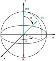
Figure 1. The Bloch sphere: a single pulse can correspond to a precise rotation on the sphere.
In superconducting architectures, qubits are driven by precisely shaped microwave pulses, typically at 4GHz to 8GHz, that are resonant with each qubit’s transition frequency. These pulses are not generic on/off signals: their shape, width, power, phase, frequency, and spectral purity determine how accurately the Bloch vector is rotated—and therefore how faithfully a quantum gate is implemented.1
Pulse Control, Readout, and Quantum Measurement
Traditionally, quantum control electronics are built from a coordinated set of functional circuit blocks: arbitrary waveform generators produce the I/Q baseband envelopes, vector signal generators supply tunable local oscillators (LOs), and I/Q mixers combine these signals into precisely shaped RF drive waveforms. In multi-qubit systems, every converter and signal source must remain locked to a common master reference clock to preserve coherence, deterministic timing, and phase alignment across the entire control stack.
While tailored microwave pulses execute quantum logic operations, computation ultimately concludes with measurement—the conversion of fragile quantum states into classical information. In superconducting architectures, this process typically relies on dispersive readout. Each qubit is coupled to a microwave resonator, and a shaped probe tone at the resonator frequency is injected into the cryostat. In the dispersive regime, the qubit’s state shifts the resonator frequency, imprinting state-dependent information onto the reflected or transmitted probe.1 That probe is then amplified, downconverted, filtered, and ultimately digitized for analysis.
At room temperature, RF ADCs acquire these weak readout signals using precisely timed capture windows. Digital downconversion, decimation, and filtering generate complex I/Q samples, which are integrated to infer the qubit state. These accurate, time-aligned measurements support real-time feedback loops that adapt subsequent control pulses and help stabilize overall processor behavior.
Because readout maps quantum information into classical signals, it becomes fundamentally limited by signal-to-noise ratio. Noise introduced by cryogenic amplifiers, converters, clocks, and other elements of the signal chain spreads the measurement outcomes in the I/Q plane, complicating state discrimination.
Taken together, pulse generation and readout form a tightly integrated control loop. High-fidelity, phase-coherent microwave pulses implement quantum gates, while a low-noise dispersive readout determines the resulting qubit states. Digital processing continuously interprets these results and refines future pulses in real time, closing the feedback loop. This convergence of precise control, reliable measurement, and deterministic synchronization is what ultimately enables scalable, practical superconducting quantum computing.
Role of Apollo MxFE AD9084 in Qubit Control and Readout
Quantum computing imposes stringent requirements on RF signal generation and measurement. Superconducting qubits operating at millikelvin temperatures demand microwave control pulses in the 4GHz to 8GHz band with ultra-low noise (<100fs rms jitter), high-spectral purity (>60dBc SFDR), and deterministic timing alignment (<10ps channel-to-channel skew) to preserve coherence and maintain gate fidelity.1
Traditional control architectures built from discrete voltage-source generators, standalone AWGs, and external mixers (Figure 2) do not scale gracefully. LO leakage degrades usable dynamic range, I/Q imbalance requires recurring calibration, increasing device count adds thermal load, and synchronizing independent instruments significantly complicates system integration. For a 1,000-qubit processor requiring three to five RF channels per qubit, the infrastructure grows to ~8,000 data converters—projecting to millions at future scales.
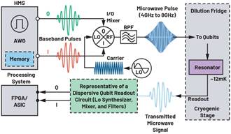
Figure 2. Discrete RF control architecture using AWGs and external mixers.
To address these constraints, the Apollo MxFE AD9084 integrates four 16-bit, 28GSPS RF DACs and four 12-bit, 20GSPS RF ADCs with on-chip digital signal processing (DSP). Direct RF synthesis and capture in the qubit band reduce board area, power per channel, and overall component count—key enablers for scalable architectures.
As a mixed-signal front end, the AD9084 is purpose-built for quantum control stacks. An on-chip PLL multiplies a low-frequency reference into a 7GHz to 14GHz sampling clock, supporting deterministic synchronization across devices. Within superconducting platforms, the AD9084 forms the interface between classical electronics and the quantum plane: FPGA-generated digital sequences become precisely shaped microwave pulses, while weak readout signals from the cryostat are captured and digitized for state discrimination and feedback. Table 1 summarizes the primary technical capabilities of the Apollo MxFE AD9084.
Table 1. Key Performance Attributes of the Apollo MxFE AD9084
| Parameter | Specification | Quantum Computing Relevance |
| DAC channels | 4 × 16-bit, 28GSPS | High-fidelity control pulse generation for qubit gates |
| ADC channels | 4 × 12-bit, 20GSPS | Low-latency qubit state readout with minimal noise |
| Analog bandwidth | Up to 9GHz (direct RF) | Covers superconducting qubit frequencies (4GHz to 8GHz) |
| On-chip DSP | NCOs, DUCs, DDCs, FIR filters, FSRC | Digital frequency conversion, pulse shaping, 30% to 50% FPGA offload |
| Synchronization | Multichip sync (MCS) with <1ps alignment | Phase-coherent multi-qubit operation across devices |
| Package | 24mm × 26mm 899-ball BGA | High-density integration for scalable systems |
By integrating RF DACs, RF ADCs, and a hardened DSP, the device supports direct RF-sampling architectures for both qubit control and readout. On-chip digital upconversion and downconversion reduce FPGA workload and simplify surrounding analog hardware.
Table 2. Typical Requirements for Qubit Control
| Parameter | Typical Requirement | AD9084 Capability | System Impact |
| Sample rate | 6GSPS to 12GSPS | 28GSPS | Direct RF synthesis with fine temporal resolution for Gaussian/DRAG pulses |
| Instantaneous bandwidth | ≥2GHz to 4GHz | 9GHz | Supports short pulses and frequency multiplexing |
| SFDR | >60dBc (in-band) | >65dBc typical | Suppresses spurious qubit excitation |
| Phase noise (integrated jitter) | <100fs rms | <50fs achievable | Preserves gate fidelity; 50fs = ~6dB SNR improvement |
| Channel alignment | <10ps skew | <1ps with MCS | Repeatable multi-qubit gate execution |
Table 3. Typical Requirements for Qubit Readout
| Parameter | Typical Requirement | AD9084 Capability | System Impact |
| Sample rate | 4GSPS to 6GSPS | 20GSPS | Direct RF readout without external mixing |
| Noise spectral density | <–155dBFS/Hz | <–157dBFS/Hz | Resolves weak state-dependent signals (1dB to 3dB differences) |
| SFDR | >65dBc | >70dBc typical | Prevents tone leakage in multiplexed readout |
| Latency | <200ns (deterministic) | <150ns achievable | Enables real-time feedback and error correction |
| Channel synchronization | <5ps | <1ps with MCS | Accurate multiplexed readout across frequency-multiplexed qubits |
Operating as the classical–quantum bridge, the AD9084 receives I/Q streams over its JESD204B/C interface. Its internal DSP performs interpolation to 28GSPS, digital upconversion via 48-bit numerically controlled oscillators (NCOs), and pulse shaping using complex finite impulse response (FIR) filters, before the 16-bit DAC cores generate analog outputs with noise spectral density below–165dBFS/Hz. This architecture minimizes external RF circuitry, improves repeatability, and supports deterministic timing—foundational for the feedback-driven loops discussed in the following section. Tables 2 and 3 summarize typical qubit control and readout requirements, respectively.
For scalable architecture, the AD9084 offers clear advantages over discrete or single-channel devices. Its 28GSPS sampling rate supports fine temporal resolution for Gaussian pulses, while four DAC channels per device reduce component count, power, board area, and clock-distribution complexity. Normal-mode operation delivers high output power in any Nyquist zone, enabling direct synthesis of 4GHz to 8GHz qubit tones without external mixers. This eliminates LO leakage, I/Q imbalance, and associated calibration overhead. The integrated fractional sample-rate converter (FSRC) provides arbitrary rate adjustments, allowing the converters to operate at optimal clocks while matching ASIC/FPGA interface rates. The inverse sin(x)/x (INVSINC) block allows improving the spectral flatness of the combined digital I/Q signal before it is sent to the RF DAC core for reconstruction. Essentially, the INVSINC block can equalize the DAC sync roll-off. However, while the loss decreases to 0 at about 90% bandwidth, correction is only possible in the first Nyquist zone.
On the receive path, resonator-based readout produces state-dependent responses that are amplified through a cryogenic high electron mobility transistor (HEMT) stage, then digitized by the AD9084’s 12-bit, 20GSPS ADCs capable of capturing wide-band frequency-multiplexed readout combs. Fine/coarse DDC stages, programmable filtering, and decimation up to 64× extract the qubit information before streaming it to the ASICs/FPGAs for integration and threshold-based classification.
Quantum computing relies on precise, phase-coherent RF control of qubits, where even small timing or phase errors can degrade system performance. In superconducting quantum systems, this demands low-noise microwave control, phase-coherent readout, and deterministic timing alignment across all qubits and operating conditions.
The Apollo MxFE AD9084 addresses this challenge with advanced MCS, providing sample-accurate alignment between its ADCs and DACs within a single device and across multiple MxFE® devices. When paired with Analog Devices’ clocking ecosystem, the AD9084 aligns internal SYSREF signals across multiple MxFEs to within ±10ps. At the system level, the ADF4030 precision clock synchronizer distributes a common master reference with sub-picosecond alignment and deterministic repeatability. For local oscillator generation, the ADF4382 frequency synthesizer integrates an ultra-low-noise VCO, achieving a –239dBc/Hz figure of merit, 31fs rms jitter at 20GHz, and a wide output range from 687.5MHz to 22GHz.
Together, coarse initialization and fine tracking calibrations, bidirectional SYSREF, and sample-accurate triggers synchronize mixed-signal and JESD204C domains across all AD9084 devices within picoseconds. With MCS tracking enabled, the ADF4382 further trims residual SYSREF timing error to below 1ps per device. Figure 3 shows a representative multidevice clocking architecture using the ADF4030 and ADF4382. This architecture delivers deterministic alignment and phase coherence across every data converter, FPGA, and Apollo MxFE devices—an essential requirement for reliable, scalable qubit control. Table 4 summarizes the impact of the ADF4382 LO performance on overall quantum system operation.
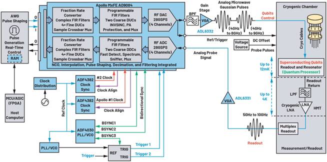
Figure 3. Block-level control/readout chain highlighting the AD9084 within a multi-qubit architecture with the ADL6331 and ADL6332.
Table 4. ADF4382 LO Generation Performance
| Parameter | Typical Value | Impact on Quantum Systems |
| Phase noise at 10kHz offset | ~–120dBc/Hz | Preserves qubit coherence times during long pulse sequences |
| Integrated jitter (12kHz to 20MHz) | <100fs rms | Enables <50fs system jitter for high-fidelity entangling gates |
| Frequency range | Up to ~18GHz | Covers both qubit control (4GHz to 8GHz) and readout bands |
| Device-to-device skew (with ADF4030) | <1ps | Coherent operation across 100+ synchronized RF channels |
This integrated architecture produces measurable system-level benefits: 30% to 50% reduction in FPGA logic by offloading digital upconverters (DUCs)/digital downconverters (DDCs), 2× to 4× reductions in JESD204 data rate through decimation, hundreds of milliwatts saved per channel, and up to 4× higher channel density relative to single-channel RF DACs. As systems evolve from prototypes toward fault-tolerant machines, the AD9084 platform enables direct RF synthesis without mixer calibration, robust multichip synchronization, flexible DSP for both ultra-low-latency feedback (<150ns) and high-fidelity waveform synthesis, and a roadmap compatible with future cryogenic integration.
Together, these capabilities make the Apollo MxFE AD9084 a compelling engine for quantum control architectures. Its combination of direct RF synthesis and capture in the qubit band, multichannel high-speed converters, deep on-chip DSP, robust synchronization, and fast profile-based reconfiguration delivers low-latency, as well as high-fidelity qubit control and readout—while providing a scalable path to large, multi-qubit systems.
Conclusion
RF data converters are the unseen engine of quantum computing—transforming digital algorithms into precise control waveforms and capturing delicate qubit responses with accuracy. The Apollo MxFE AD9084 brings this role into focus: high sample rates, wide direct-RF bandwidth, deterministic low latency, and tight multichannel synchronization in a single, integrated platform. Paired with deterministic clocking (ADF4030) and low-phase-noise LO synthesis (ADF4382), it reduces component count, removes mixer-calibration complexity, enables phase-coherent scaling, and offloads substantial FPGA workload as systems grow. As the industry moves toward larger qubit counts and cryogenic integration, platforms that consolidate performance, power efficiency, and intelligence at the edge will define the next wave of breakthrough quantum machines—and the AD9084 is built to lead that journey.


