


Wide band gap (WBG) semiconductors have been a ‘hot’ topic for some years now and have firmly transitioned from being tomorrow’s technology to being a major market sector in their own right, with growth of the market predicted to be 33.4% CAGR over the next five years to US $1.82B by 2024 [1]. WBG devices are fabricated using either Silicon Carbide (SiC) or Gallium Nitride (GaN) materials with SiC the largest proportion by far – about 98% in 2018 according to researchers Yole Développment [2]. They predict the main market driver to be automotive, with SiC about 50% share of semiconductor power switches in 2024. So, what do we mean by ‘wide band gap’ devices? They are semiconductors fabricated with materials that exhibit the characteristic that relatively high energy is needed to move electrons from an atomic ‘valence’ band to its ‘conduction’ band. This ‘band gap’ is measured in electron-volts (eV) and as a comparison, the value for traditional silicon (Si) is 1.1eV, SiC is 3.26eV and GaN is 3.4eV. WBG devices also have better electron saturation velocity and SiC particularly has very good thermal conductivity. These and other differences, compared with Si in Figure 1, result in some properties that give considerable benefits for W BG devices.
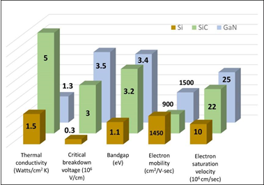
Figure 1: SiC and GaN material characteristics compared with Silicon
WBG device have 10x better breakdown voltage rating
As seen in Figure 1, with around 10x better voltage breakdown characteristics for a given thickness than Si, devices using SiC materials, for example, can have a 10x thinner drift layer with 10x the doping concentration. This yields much lower on-resistance than Si for the same blocking voltage which also directly results in lower dissipation for the same die area compared with Si. With its extremely high thermal conductivity, a SiC die can lead heat dissipation effectively out of the component package allowing high power in minimal space. Leakage currents are also lower as a consequence of the high voltage breakdown characteristic, especially at high temperatures.
Small size equals low capacitances and high speed The small die size achievable with high blocking voltage with WBG semiconductors produces low internal device capacitances. In switching applications, capacitances must be charged and discharged each cycle, representing circulating current and power dissipation, so again, SiC and GaN have a big advantage over Si. Gate charge for example, due to gate to source and gate to drain capacitances can be several microcoulombs in IGBTs and hundreds of nanocoulombs for power MOSFETs but for a SiC device it is just tens of nanocoulombs, even for high power devices such as the FF45MR12W1M1_B11 from Infineon, rated at 1200V and 25A (Figure 2). This not only aids fast switching but also keeps gate drive power requirements down – large IGBTs can need several watts to drive their gates while it’s typically milliwatts for SiC and GaN.
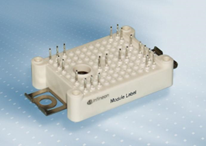
Figure 2: SiC module from Infineon rated at 1200V/25A with just 62nC total gate charge
High temperatures are possible with WBG devices
One of the useful features of SiC and GaN is their ability to work at higher junction temperatures than Si. Some manufacturers have shown their devices to work at peak temperatures over 500°C though practically, packaging limits values to those seen with silicon parts. The better ratings though give a large margin under transient thermal conditions with WBG devices. Variation of critical parameters with temperature such as on-resistance and gate leakage are also much lower with SiC compared with Si.
Application benefits
The main driver for using WBG devices is lower loss in switching applications. Efficiency targets for applications such as server power supplies are now routinely over 98% and these values can only practically be achieved with SiC or GaN technology. Optimum solutions are not however achieved when older technology such as Si-MOSFETs are simply replaced with SiC for example: edge rates will be faster, giving lower losses in the device, but EMI will also be considerably higher requiring extra snubbing and filtering which adds losses back in. Full benefit is achieved with ground-up redesigns that increase the operating frequency to a point where switching losses are still low but savings are achieved also in external components, particularly magnetics, which generally scale down in size and cost as frequency increases. With higher operating frequencies, board layout is also critical. An optimum solution will depend on cost, size and weight targets as well: automotive electric motor drive applications for example, put a premium on efficiency, size and weight which potentially extends driving range. External components are not so much affected in the application as the ‘magnetics’ involved are the motor windings, which are scaled for torque and power rather than switching frequency. For this reason, motor drive switching frequencies are not pushed too high.
In industrial drive applications, weight may not be an issue but efficiency and size improvements can allow more drives to be fitted in a cabinet, potentially saving valuable factory floor space and increasing productivity.
Design considerations
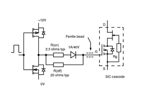
When designing with WBG devices, there are some considerations to be aware of. Gate drive voltages are critical for optimum switching performance and vary between types: Littelfuse (IXYS) for example, recommend +20V/-5V operational values and +22V/-6V maximum for their SiC MOSFET device LSIC1MO120E0080. According to the data sheet, gate threshold voltage can be as low as 1.8V but for lowest on-resistance, 20V should be applied. Devices will be off when 0V is applied to the gate but a negative voltage is typically recommended to offset transient effects caused by the extremely fast di/dt in the source connection, which reacts with source package and interconnection inductance to produce voltage transients which can spuriously turn the device on. WBG devices will switch in nanoseconds but many practical designs will deliberately slow switching edge rates with series gate resistors and ferrite beads to avoid EMI and high di/dt issues (Figure 3).
In many applications such as bridge circuits in inverters, ‘commutation’ occurs, that is, current flow in the reverse direction in switches, caused by inductive loads. For IGBT circuits, a parallel diode is necessary to allow commutation but in MOSFETs a body diode is inherent and can replace the external diode in some circumstances. For Si-MOSFETs, the diode is relatively slow and drops high voltage so is not efficient. For a SiC MOSFET, the diode is much faster, but still has a relatively high forward voltage drop (3.3V) compared with a fast Si diode. GaN devices have no body diode but can conduct through their channel in the reverse direction but with no reverse recovery charge.
Devices available
For very high frequency applications, to avoid parasitic effects, leadless surface-mount types are preferred such as the PG-HSOF-8-3 package favoured by Infineon for their GaN devices. Most suppliers though offer parts in leaded TO-247 packages for ease of heatsinking and to offer an easy upgrade path from an earlier technology such as IGBTs or Si-MOSFETs in the same package. Common devices are normally-off SiC MOSFETs but normally-on SiC JFETs are also available. Some suppliers such as UnitedSiC offer cascodes – a combination of SiC JFET and Si-MOSFET. These devices have the temperature and speed advantages of SiC but with the ease of gate drive of an Si-MOSFET. They do not have a body diode, but conduct in the reverse direction with low voltage drop and no reverse recovery. They are also available in ‘stacked’ versions for higher voltage operation.
Applications
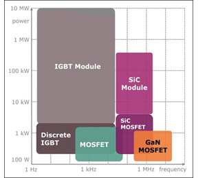
SiC semiconductors are firmly established in AC-DC power supplies in power factor correction and conversion stages; data centres are a major driver with their requirement for higher power density and energy savings. SiC is now common in motor drives and inverters generally, with EV chargers a main application. Traction inverters in EVs and other areas such as rail are also transitioning away from IGBTs to SiC. Other technologies have their place but SiC is set to dominate at higher frequencies and over a wide power range (Figure 4).
SiC devices mentioned and many more are available from distributor TME Electronic Components [3] from stock.


