


Introduction
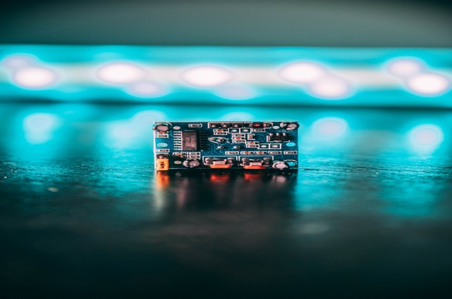
Printed Circuit boards (PCBs) handle supplying electrical connection between the different components of a motherboard. They are used in all the electronic devices. The PCBs are manufactured in different thicknesses depending on the specifications of the motherboard in which they are installed.
In this article we are going to discuss two diverse types PCBs. In the first part of the article you are going to read about standard thickness of PCBs along with designing and assembling factors that affect the thickness of standard PCBs.
In the later part of the article, you will read about advantages of thick copper PCBs and factors to consider if you are thinking of customized thickness. Towards the end of the article you will get a balanced comparison between Standard PCBs and thick Copper PCBs.
Standard Thickness of PCBs
When you think of the word standard a benchmark might come to your mind. For example, Cadillac was being used as a benchmark for automobiles. Standard is also referred as criteria that must be followed by the manufactures of a certain product. For example, the stand size for a couch built for three people is 84 inches. Similar is the case for standard of PCBs, there are certain dimensions and functions that must be present in a PCB.
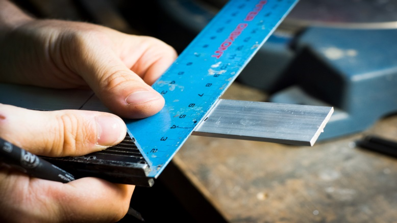
The standard thickness of PCB is 1.57mm or 0,062 inches. The standard was set back in the days when Bakelite sheets were manufactured during the early days of board fabrication, since then the standard has stuck. Therefore, the standard can be called as historical standard. The dimensions on which boards are being manufactured today are different from the standard dimensions. Today boards are larger as well as smaller than this standard.
The size of PCB can vary depending upon your choice of copper board fabrication and aligning method.
There are number of designing and assembling factors that affect the thickness of PCBs.
Design factors that affect the thickness of PCB
- Diameter of copper
- Design of material
- Number of PCB layers
- Types of Vias
- Operating environment.
Assembling factors that affect the thickness of PCB
- Drill hole equipment
- Copper width
- Layer count
- Depenalization method
Thick Copper PCBs
The thick copper PCBs are much in demand in boards that are used in the devices of telecommunication sector. As the thick copper PCBs are efficient in transmitting higher values of current thus, they are best suitable for the telecommunication devices.

Thicker copper PCBs are designed for heavier duties.
Thick copper PCBs are an important part of our lives and many of the daily activities of our life would not have been possible without the thick copper PCBs.
The manufactures design the boards to meet the requirements of the devices in which are to be used.
Advantages of using thick Copper PCBs
- As the thick Copper PCBs have higher copper used in them therefore, they are efficient in conducting higher current values
- The thermal distribution is better in thick copper PCBs.
- They mechanical strength of thick copper PCBs is much efficient.
- They can sink heat therefore they provide better performance with getting heated.
- By using the thick copper, the anti-stress ability of the board can be increased because the PCBs can withstand the thermal stress.
- Thick copper PCBs can improve the mechanical resistance of joints between the layers.
Factors to Consider for customized thickness
If you are planning to have a custom thickness for a PCB you might have questions in your mind about custom thickness of it? Below are some factors which you should consider before opting for customized PCB
CM’s equipment capability
The first thing to consider is whether your CM has the capability of producing the diameter which you require? Before the designing process of your board, this determination shall be made otherwise you will be forced to redesign the layout.
Extended turnaround time
There are some common thickness sizes which are easily available in the market however if your desired thickness size is uncommon in the market it might affect your development quality and delivery schedule so before you decide a thickness size for your PCB you must check its availability in the market.
Additional cost
You should also consider the added charges for extra specialized materials which will be used for manufacturing the PCBs and the manpower that will be needed. You should only choose customized thickness if and only If the added cost if bearable to you.
At times it is better to go with standard thickness because the standard designs are already available in the market and the extra time will be needed to manufacture the custom PCBs.
Comparison between Standard PCBs and thick copper PCBs
| Standard PCBs | Thick Copper PCBs |
| The measurement unit for standard PCBs is ounces (oz). The amount of copper used in these PCBs is 1oz therefore they have thin size. | The Thick copper PCBs have thicker diameter than the Standard size because higher amount of copper is used in them. The measurement unit for thick copper PCBs is ounces (oz). The amount of copper used in them is 2oz to 4oz |
| Copper etching and platting method is used for the manufacturing of standard PCBs | Thick copper PCBs are manufactured through step platting and differential etching. |
| Standard PCBs are manufactured to perform lighter activities | Thick copper PCBs are designed to perform heavy duties |
| They Conduct lesser amount of current | Can conduct higher values of current |
| The thermal distribution is not as efficient as thick copper PCBs | Thermal distribution is efficient in Thick copper PCBs therefore they are efficient in performance |
| Standard PCBs have lesser mechanical strength as compared to Thick copper PCBs | As more copper is used in them therefore, they have better mechanical strength |
| The standard PCBs do not enhance the ability of board in which they are used | The anti-stress capability of the Board can enhance using thick copper PCBs |
- In the past, these copper type PCBs were made through etching thick coper clad but with the advancement of technology, they are made with the combination of plating and etching.
- This technological advancement has helped the manufactures in reducing the size of PCBs by cutting the extra edges and side wall of the boards.
- In the past high-power circuit and control circuits were made on different boards but now they are combined.
- The usage of heavy copper platting has made it possible for the high current circuits to have simple board structures.
- Heavy copper circuits are ideal because they can be easily linked to the standard circuit boards.
To learn more about PCB and thick copper PCB, you can browse the website:https://www.pcbonline.com/


