

Introduction
Printed circuit board assembly (PCBA) is at the heart of modern electronics, connecting the worlds of PCB fabrication and product completion. Whether building a PCB prototype for validation or scaling up to high-volume electronics manufacturing, a reliable PCB assembly process is crucial for product performance, safety, and time-to-market. From the simplest single board to multi-layered, high-density PCB assemblies for aerospace, mastering the assembly process and board design can mean the difference between success and costly failure. In this comprehensive guide, we’ll cover the PCBA process, the role of various components, PCB design files, assembly methods, inspection techniques, and provide valuable tips for engineers and procurement teams.
What is PCB Assembly and PCBA?
PCB assembly is the process of soldering or assembling electronic components onto a bare PCB (printed circuit board). This transforms the static, copper-laden substrate into a completed PCBA—an engaged, fully functional board at the core of every electronic device.
PCBA (Printed Circuit Board Assembly) refers to the final product where all electronic components have been securely attached, tested, and verified on the assembled board. With the rise of complex circuit boards, the PCBA manufacturing process has grown to include various assembly methods—SMT (surface mount technology), through-hole components, and now mixed assembly that leverages both for maximum performance.
PCB vs. PCBA
- PCB: The bare board made of layers of substrate, copper traces, solder mask, and silkscreen, fabricated through a detailed manufacturing process.
- PCBA: Represents assembled PCB boards after mounting various components, solder joints, and conducting all necessary inspection and testing steps.
Printed circuit board assemblies enable virtually every electronics device, from smartphones to satellites, by supporting the process of mounting and soldering electronic components onto a PCB.
PCB Design and Preparation
PCB design is the foundation of the entire assembly. The board design phase must anticipate the requirements of assembly and inspection as much as its electrical performance.
- PCB design files include Gerber files for copper, solder mask, silkscreen, and drilling, a BOM (bill of materials) listing all required components, and a CPL or pick and place file for component placement.
- Material of a PCB: Often FR4 for standard, rigid boards; polyimide for flex PCBs; or specialized substrates for demanding environments.
- A well-prepared board layout incorporates DFM (Design for Manufacturing) and DFA (Design for Assembly) best practices, including adequate spacing, test points, optimized pad shapes, and provision for both SMT and through-hole assembly.
- Modern PCB manufacturers also perform thorough DFA checks, reviewing for manufacturability and cost optimization before starting the PCB fabrication and assembly journey.
Step-by-Step PCB Assembly Process (PCBA Process)
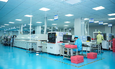
The journey from bare board to completed PCBA involves a blend of automation, precise inspection, and skilled craftsmanship.
DFA and Pre-Assembly Setup
Kit Audit & File Verification:
- The PCBA process begins by verifying that all required components are accounted for (BOM matched), incoming quality of materials checked, and PCB design files have no discrepancies.
- DFA review helps catch issues such as improper footprints or missing solder mask openings before expensive production starts.
Stencil Fabrication:
- Especially for surface mount components, a stencil matching the PCB’s SMD pads is fabricated for accurate solder paste deposition.
SMT Assembly Process
Solder Paste Application:
- Solder paste is applied to the board using the SMD stencil. Quality here is vital; poor solder paste application is the main cause of faulty solder joints.
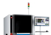
- 3D SPI (Solder Paste Inspection) scanners offer precise analysis, allowing rapid correction if the solder paste is misapplied.
Pick and Place Process:
- An automated process uses pick-and-place machines to place small components, ICs, and SMD passives onto the deposited solder paste per the CPL file.
- The accuracy of component placement is verified in real time, ensuring functional assembly and preparedness for mass production.
Reflow Soldering:
- Boards travel through a reflow oven, where temperature profiles are tuned to melt the solder paste—creating robust solder joints for all surface mount components.
- For double-sided PCB assemblies, the process is done in stages, carefully monitored to prevent damage or movement of previously mounted parts.
Inspection:
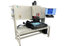
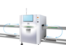
- AOI (Automated Optical Inspection) machines scan each board for orientation errors, missing parts, misaligned components, and solder joint issues.
- X-ray inspection is used for BGAs, QFNs, and other leadless packages where solder joints aren’t visible on the PCB surface.
Through-Hole Component Assembly
- Through-hole components are inserted into drilled holes and soldered, often using wave soldering or selective soldering depending on board layout and density.
- Manual soldering is reserved for delicate parts, non-washable components, or additional assembly after cleaning.
- Mixed assembly allows the same PCB to benefit from the density of SMT and the ruggedness of through-hole assembly.
Through-hole components with leads or wires—like connectors or large capacitors—still play a vital role in PCB manufacturing, despite the dominance of SMT.
Cleaning and Post-Assembly Services
- After SMT and THT assembly, PCBs are cleaned to remove flux residues using deionized water or specialty solvents.
- A clean assembled board not only looks professional but also prevents leakage current, corrosion, or electrochemical migration common in exposed circuits.
Final Inspection, Testing, and Packaging
- Every PCB goes through final inspection—often both manual and automated—with detailed checking for solder bridges, opens/shorts, missing parts, or incorrect polarities.
- In-circuit and functional testing validate the assembled PCBA against the original board design.
- Once passed, PCBs are packed in ESD-safe packaging, boxed, and labeled per customer requirements. Complete traceability is maintained from PCB fabrication to completed assembly.
Conformal Coating and Protection
- For industrial, automotive, medical, or aerospace applications, a protective conformal coating is applied, insulating the circuit against moisture, dust, and chemicals.
Mixed Assembly and Advanced PCBA Methods
Mixed assembly, which uses both SMT and through-hole components, is now common for printed circuit board assemblies requiring mechanical support and high component density.
- Mixed assembly methods include assembling electronic components onto both sides of the PCB, integrating SMT and THT in panelized builds, and using adhesives or weird assembly profiles when necessary.
- Box build assembly: PCBA services often extend to integrating the assembled PCBA into enclosures with connectors, cables, and final product assembly (full electronic assembly).
Automated PCB assembly lines now combine multiple pick-and-place heads, SMT and THT section handoffs, and real-time AOI feedback for uninterrupted, high-yield circuit assembly.
Tips for PCBA Designs and PCB Assembly Quality
- Standardize Component Packages: Keeping SMD sizes (0603, 0805, SOIC) uniform streamlines BOM management and sourcing.
- Include Test Points: Easier inspection and in-circuit test = faster troubleshooting and higher PCBA quality.
- Pad and Mask Optimization: Avoid via-in-pad where possible, adequately space high-current traces, and keep copper balanced to prevent warping.
- Panelization: For small PCBs, panelize for maximum line efficiency and fewer handling errors.
- Prototyping Smartly: Begin with a well-crafted PCB prototype assembly using a local or rapid-turn PCB assembly service. Early functional boards catch design faults cheaply and allow you to iterate PCB design, layout, and circuit configuration before moving to mass PCB manufacturing and assembly.
- Component Sourcing and BOM Hygiene: Use only authorized, traceable suppliers for all electronic components. List valid alternates in your BOM for at-risk ICs. When preparing for PCBA manufacturing, ensure your BOM is checked against global supply chain databases to pre-empt shortages that could stall your product assembly.
- Soldering or Assembling Electronic Components: Whether SMT, through-hole, or mixed assembly, ensure the process of soldering electronic components onto each bare PCB—via reflow soldering, wave soldering, or selective hand soldering—matches component and circuit board requirements.
PCB Assembly Services and Industry Applications
Every sector—automotive, consumer electronics, medical, industrial, research, or defense—relies on reliable PCB assembly services for their functional board builds. Here’s how top industries apply and demand high standards from PCBA:
- Automotive PCBs: Withstand vibration, temperature swings, and moisture. Rigorous inspection and robust assembly process (often box build assembly) are critical.
- Medical PCBs: High reliability, complete traceability, and extensive functional testing on completed PCBA are mandatory to meet ISO 13485 and IPC-A-610 Class 3.
- Aerospace/Defense: Often require mixed assembly (SMT and thru-hole), thorough inspection, burn-in testing, and full materials traceability for all printed circuit board assemblies.
- Consumer Electronics: Prioritize speed, cost, and high-volume production. Automated PCB assembly with dense SMD population and rapid box build assembly is common.
- Industrial, IoT, and Research PCBs: Often call for low- or mid-volume, flexible PCBA services that can adapt to evolving circuit designs and frequent PCB prototype revisions.
PCB Assembly Cost and Troubleshooting
Understanding the factors impacting PCB assembly cost will help you budget and optimize product assembly for various volumes and product complexities.
Key Cost Drivers:
| Factor | Typical Impact |
| Board Size/Layer Count | More layers/traces mean higher cost for fabrication and assembly. |
| Component Count/Type | High pin-count, fine-pitch, or BGA/QFN raise placement and inspection demands. |
| SMT vs. Thru-Hole Mix | Combined/mixed assembly steps are more complex and usually more costly. |
| Testing/Inspection Required | Increased AOI, X-ray, or functional tests add incremental cost. |
| Volume (Prototype → High Volume) | Per-unit costs drop as batch size increases. |
| Turnaround Time | 24-hour pcb prototype builds may cost more than standard schedules. |
Troubleshooting & Common Defects:
| Defect | Likely Cause | Prevention/Troubleshooting |
| Solder Bridges | Excess solder paste, pad design | Tune stencil and SPI; adjust pad widths; use AOI. |
| Tombstoning | Asymmetry in pads or thermal gradient | Correct footprint/pad size; tweak reflow oven profile. |
| Voids (BGA/QFN) | Outgassing, poor solder paste | Use vacuum in reflow; optimize stencil and placement. |
| Open Circuits | Missing solder or component | Ensure SPI, AOI, and in-circuit testing closure. |
| Cold Joints | Low oven temps, bad paste | Confirm reflow profile; ensure fresh paste is used. |
If an assembled PCB fails functional or electrical test, isolate faults via ICT or FPT, review the process of mounting, and check both the bare board and pcba steps in the pcba. Defects can be traced back to solder paste application, pick and place process, or errors in PCB design files.
Conclusion
The journey from bare board to completed PCBA is a sophisticated mix of design foresight, precise PCB fabrication, advanced PCB assembly process control, and best-in-class inspection. The choices you make—from component sourcing, through pcb design and board layout, to choosing your automated PCB assembly partner—ultimately shape every electronic device’s performance and lifecycle.
Key Takeaways:
- Start with robust, DFM/DFA-optimized PCB design and layout, and clear documentation.
- Lean on automated and mixed assembly methods with strong inspection—AOI, X-ray, SPI—for every production process step.
- Use PCBA services that can scale from rapid PCB prototype builds to volume production, while offering inspection, testing, and box build assembly integration.
- Always verify pcba quality by comprehensive inspection, and plan for both initial yield and long-term reliability regardless of industry, whether it’s consumer electronics or printed wiring board assemblies for mission-critical medical or aerospace devices.
Your path to reliable, scalable, and efficient circuit assembly requires understanding both the art and science behind PCB and PCBA manufacturing. With the right approach, every assembled PCB becomes the building block for innovation in today’s fast-moving world of electronics manufacturing.
FAQs About PCBA Assembly
1. What does PCBA stand for?
PCBA stands for Printed Circuit Board Assembly. It refers to a PCB that has electronic components mounted and soldered onto the board.
2. What does PCB assembly do?
PCB assembly installs and connects electronic components onto a bare PCB using SMT, through-hole, or mixed assembly processes to create a functional electronic circuit.
3. What is the difference between PCB and PCBA?
A PCB is a bare printed circuit board without components. A PCBA is the completed board after electronic components have been assembled and soldered onto the PCB.
4. How much does it cost to assemble a PCB?
PCBA assembly cost depends on board complexity, component count, order quantity, SMT/THT processes, component sourcing, testing, and special manufacturing requirements.
5. Is PCBA assembly expensive?
Not necessarily. Standard SMT assembly can be cost-effective, while BGAs, fine-pitch components, low-volume orders, complex testing, and special processes can increase the assembly cost.
6. How long does PCB assembly take?
PCBA lead time depends on component availability, order quantity, board complexity, assembly process, and testing requirements. Prototype orders are generally faster than volume production.
7. What is the function of a PCBA board?
A PCBA provides the electrical and mechanical platform that connects electronic components and enables the finished device to perform its intended functions.
8. What are common PCBA assembly problems?
Common PCBA defects include solder bridges, insufficient solder, tombstoning, component misalignment, open joints, BGA voids, polarity errors, and component damage.
9. Why do PCB assemblies fail?
PCBA failures can result from poor solder joints, incorrect components, contamination, thermal stress, moisture, design issues, component defects, or inadequate process control.
10. How can you tell if a PCBA is faulty?
A faulty PCBA can be identified through visual inspection, AOI, X-ray inspection, ICT, flying probe testing, and functional testing, depending on the board design and application.