


Abstract
Self-driven synchronous rectification can improve efficiency in active-clamp forward converters while avoiding isolated secondary-side gate drivers. This article reviews the operating principles and highlights practical limitations of conventional self-driven schemes. Simple circuit modifications are presented to extend usable operation to both higher- and lower-output-voltage designs. Measured application examples using active-clamp forward controllers are included to illustrate real-world performance and design trade-offs.
Introduction
The growing demand for high-current, low-voltage power supplies in applications such as telecommunications infrastructure, data centers, industrial automation, and automotive electronics places significant emphasis on efficiency, thermal performance, and power density. As load currents continue to trend upward, power losses associated with output rectification increasingly dominate the overall converter efficiency. In many isolated DC-to-DC converter designs, the rectifier diodes on the secondary side become a primary bottleneck, limiting both current capability and achievable thermal performance.
One of the most effective methods to address rectifier loss is synchronous rectification, where power MOSFETs replace diodes on the secondary side of the transformer. The resulting efficiency improvement directly translates into reduced power dissipation, improved thermal margins, and the ability to deliver higher continuous output current.
Despite these advantages, synchronous rectification introduces several implementation challenges in isolated converter architectures. Among those is the need to generate appropriate gate-drive signals for the secondary-side MOSFETs while maintaining isolation from the primary controller. Conventional solutions employ dedicated isolated gate drivers or complex control circuits on the secondary side, both of which increase cost, complexity, and component count.
For converter topologies with a limited input-voltage range—typically no more than 2× variation—self-driven synchronous rectification provides an elegant and low-cost alternative. In this approach, the gate-drive signals for the synchronous rectifiers are derived directly from transformer secondary voltages, eliminating the need for dedicated driver ICs. When combined with the active-clamp forward converter topology, self-driven rectification becomes particularly attractive, as the reset waveforms naturally provide square wave voltages suitable for directly driving MOSFET gates.
This article examines the principles of self-driven synchronous rectification as applied to active-clamp forward converters. It describes the basic operating mechanisms, identifies key limitations of conventional implementations, and presents practical circuit modifications that extend the usable output voltage range. Tested application examples using Analog Devices’ active-clamp forward controllers are discussed to illustrate real-world performance and design considerations.
Overview of the Active-Clamp Forward Converter
The active-clamp forward converter is an evolution of the conventional single-ended forward topology, designed to improve efficiency and reduce voltage stress on the primary-side switching devices. In a traditional forward converter, transformer reset is typically accomplished using either a third reset winding or a resistor-capacitor-diode (RCD) clamp network. While functional, these approaches dissipate magnetizing energy and impose significant voltage stress on the primary switch. In contrast, an active-clamp forward converter employs an active reset circuit consisting of a clamp capacitor and an auxiliary switch, typically a MOSFET, connected across the transformer’s primary winding. During the main switch on-time, energy is transferred from the primary side to the secondary side, supplying the load while magnetizing current builds in the transformer core. When the main switch turns off, the clamp switch turns on, allowing the magnetizing current to resonate with the clamp capacitor. This resonance resets the transformer flux while recycling stored energy back into the power path rather than dissipating it as heat.
This active reset mechanism provides several compelling advantages.
- Reduced primary switch voltage stress: The clamp capacitor limits the peak drain-to-source voltage of the main MOSFET, enabling the use of lower-voltage devices with improved conduction performance.
- Zero-voltage switching (ZVS): The resonant transitions between the main and clamp switches can achieve ZVS over a wide operating range, significantly reducing switching losses.
- Improved electromagnetic interference (EMI) performance: Soft switching and controlled voltage transitions reduce high-frequency noise generation.
- Higher maximum switching frequency: Lower switching losses enable operation at higher frequencies, supporting increased power density.
Due to these characteristics, active-clamp forward converters occupy a favored position between simple flyback converters and more complex resonant topologies. They are widely used in medium- to high-power isolated applications where efficiency, reliability, and thermal management are critical design requirements.
Analog Devices Active-Clamp Forward Controllers
The LT3752/LT3752-1 and LT3753 are highly integrated, high-performance active-clamp forward controllers that minimize external component count, solution size, and cost. All three parts produce compact, versatile, and efficient solutions for single-IC output power levels up to 400W. Higher power levels can be achieved by stacking converter outputs in series.
The LT3752/LT3752-1 include an internal constant-frequency flyback controller for generating a housekeeping supply. The housekeeping supply can efficiently provide bias for both primary and secondary ICs, eliminating the need to generate bias supplies from auxiliary windings in the main forward transformer, significantly reducing transformer complexity, size, and cost.
The housekeeping supply can be used to overdrive the INTVCC pin to take power outside of the part, improve efficiency, provide additional drive current, and optimize the INTVCC level.
The LT3752 is designed for input voltages up to 100V, making it suitable for applications such as telecom intermediate bus converters and industrial power supplies. The LT3752-1 extends the operating range beyond 100V, targeting high-voltage automotive battery systems and offline isolated power supplies. The LT3753 offers additional flexibility for low-voltage, high-current designs.
These controllers provide several features that simplify active-clamp forward designs, including programmable switching frequency, current-mode control for fast transient response, accurate programmable volt-second clamp, and robust protection features. When combined with self-driven synchronous rectification on the secondary side, they enable highly efficient isolated power solutions with minimal component count.
Self-Driven Synchronous Rectification Principles
Basic Concept
In a self-driven synchronous rectification scheme, the gate-drive signals for the secondary-side MOSFETs are derived directly from voltages induced on the transformer secondary windings. Because these voltages are inherently synchronized with primary-side switching activity, they provide natural timing for turning the synchronous rectifiers on and off without requiring additional control logic.
In an active-clamp forward converter, the transformer secondary produces two key voltages.
- Forward Switch Waveform (FSW): Corresponds to the conduction interval of the main forward switch.
- Clamp Switch Waveform (CSW): Corresponds to the conduction interval of the clamp switch during transformer reset.
These waveforms resemble square waves and are well suited for driving MOSFET gates directly. By appropriately connecting the gates of the synchronous forward MOSFET and synchronous catch MOSFET to these signals, each device conducts during the correct portion of the switching cycle, mimicking the behavior of traditional diode rectifiers with substantially lower conduction loss.
Example Application
Figure 1 illustrates a 5V, 20A active-clamp forward converter designed for a 36V to 72V input range. In this example, the active reset circuit consists of a P-channel MOSFET, M2, and a reset capacitor, C7. The clamp capacitor voltage automatically adjusts with the duty cycle to ensure complete transformer reset under all operating conditions.
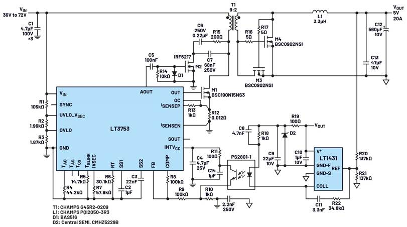
Figure 1. 5V, 20A active-clamp forward converter designed for a 36V to 72V input range with self-driven synchronous rectification with the LT1431.
Because the reset waveform is approximately square in shape, it can be used directly as a MOSFET gate-drive signal on the secondary side. Figure 2 shows the resulting CSW and FSW waveforms used to drive the forward and catch synchronous rectifiers, respectively.
This arrangement eliminates the need for secondary-side controllers or isolated drivers, significantly reducing cost and design complexity while achieving high efficiency.
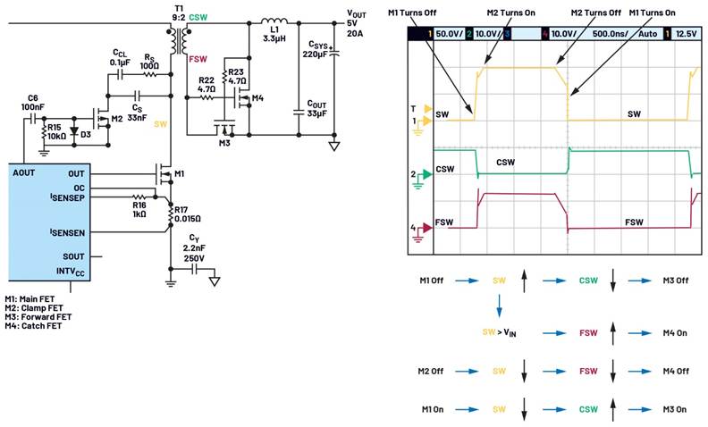
Figure 2. Self-driven synchronous rectification waveform.
Limitations of the Conventional Self-Driven Scheme
Although self-driven synchronous rectification offers compelling advantages, the conventional implementation has inherent limitations tied to its dependence on the transformer’s secondary voltage. Specifically, the gate-drive voltage applied to the secondary MOSFETs is proportional to the output voltage of the converter. This dependency creates two problematic operating regions.
- High output voltage (>5V): The induced gate-drive voltage may exceed the maximum VGS rating of the MOSFETs, risking long-term reliability or immediate device failure.
- Low output voltage (<2.5V): The available gate-drive voltage may be insufficient to fully enhance the MOSFETs, resulting in high conduction losses and degraded efficiency.
Figure 3 illustrates this limitation, showing how the gate-drive amplitude scales with output voltage in a conventional self-driven design. To ensure reliable operation across a broader range of output voltages, the basic topology needs to be modified.
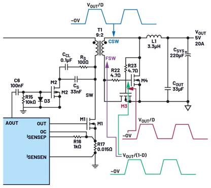
Figure 3. The gate-drive amplitude scales with output voltage in a conventional self-driven design.
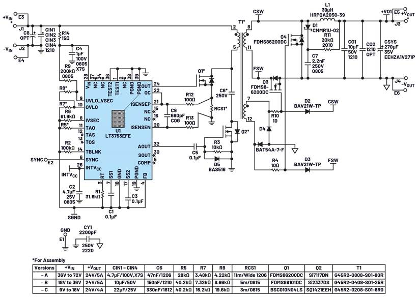
Figure 4. This 24V output self-driven forward has a simple modification that extends the applicability of self-driven synchronous rectification to high output voltages using the DC2324A.
Modified Self-Driven Scheme for High Output Voltage Applications
When the converter output voltage exceeds approximately 5V, the primary concern becomes limiting the gate-to-source voltage applied to the synchronous rectifier MOSFETs. A straightforward solution is to introduce an auxiliary secondary winding on the transformer dedicated to gate drive.
By carefully choosing the turns ratio of this auxiliary winding, a scaled-down version of the secondary voltage can be generated, ensuring that the MOSFET gate drive remains within safe operating limits. As shown in Figure 4, this auxiliary winding supplies the gate-drive voltage for both the forward and catch MOSFETs.
In this configuration, diodes connected to the CSW and FSW nodes provide a reliable means of turning off the MOSFETs at the appropriate times. Because the auxiliary winding voltage is lower than the main secondary voltage, the diodes remain reverse-biased during normal operation, preserving correct switching behavior.
This simple modification extends the applicability of self-driven synchronous rectification to higher output voltages without introducing significant complexity or cost.
Modified Self-Driven Scheme for Low Output Voltage Applications
Low output voltage designs present a different challenge. When VOUT falls below approximately 2.5V, even a turns-ratio-optimized secondary winding may not provide enough voltage to fully enhance the synchronous rectifier MOSFETs. In this case, simply adding an auxiliary winding is insufficient, as the behavior of the steering diodes changes and proper biasing cannot be maintained.
To address this limitation, the modified scheme shown in Figure 5 introduces additional small-signal MOSFETs and an inductor to shape and amplify the available gate-drive voltage. These components effectively decouple the gate-drive amplitude from the output voltage while preserving correct timing derived from the transformer waveforms.
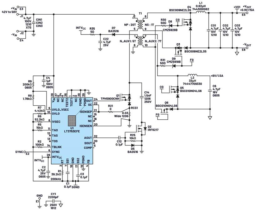
Figure 5. This 0.9V, 15A output self-driven forward converter enables efficient synchronous rectification in ultra-low-voltage, high-current applications.
This approach enables efficient synchronous rectification in ultra-low-voltage, high-current applications—for example, A 0.9V, 15A output converter—where diode losses would otherwise be prohibitive. Although this solution adds modest complexity, it remains significantly simpler and more economical than implementing a fully controlled secondary-side driver circuit.
Practical Design Considerations
When implementing self-driven synchronous rectification, several practical aspects must be carefully considered.
- MOSFET selection: Devices should have low RDS(ON), appropriate VGS ratings, and fast intrinsic diodes to minimize reverse recovery losses during switching transitions.
- Transformer design: Winding placement, leakage inductance, and coupling all influence waveform integrity and timing. Auxiliary windings must be carefully optimized for accurate voltage scaling.
- Dead-time control: Although self-driven schemes inherently provide correct timing, parasitic delays can result in brief cross-conduction or body-diode conduction. Proper layout and component selection help mitigate these effects.
- Startup behavior: During startup and light-load conditions, the available gate-drive voltage may be reduced. Ensuring stable operation in these modes is essential for robust designs.
Careful attention to these details ensures that the efficiency gains promised by synchronous rectification are fully realized in practical implementations.
Conclusion
Self-driven synchronous rectification offers a powerful means of improving efficiency and current capability in active-clamp forward converters while minimizing cost and complexity. By leveraging transformer-derived waveforms, designers can eliminate the need for dedicated secondary-side drivers and achieve highly efficient isolated power supplies.
While the conventional self-driven scheme is limited to a narrow output voltage range, simple and effective modifications can extend its applicability to both high-voltage and low-voltage outputs. When combined with Analog Devices’ active-clamp forward controllers, these techniques enable compact, high-performance solutions well suited to modern power conversion challenges.