

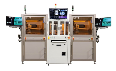
Sono-Tek SPT300WS Ultrasonic Coating System – Sono-Tek Corporation will introduce its new SPT300WS automated ultrasonic photoresist coating system at SEMICON Europa, November 10-13, 2026, at Messe München in Munich, Germany. The system will be exhibited in Sono-Tek Booth C1.254.
Developed for precision semiconductor manufacturing, the SPT300WS expands Sono-Tek’s automated wafer-coating platform to provide standard processing capability for wafers up to 300 mm. The fully enclosed system is designed for photoresist and protective coating applications, including MEMS, advanced packaging and wafers with deep wells, high-aspect-ratio features or other challenging three-dimensional topographies.
The SPT300WS incorporates automated wafer-shuttle capabilities similar to Sono-Tek’s established SPT200WS platform. The automation is designed to transfer wafers between the cassette, pre-alignment station and coating module, reducing operator involvement and supporting repeatable production processing.
“The SPT300WS represents an important expansion of our semiconductor coating platform,” said Steve Harshbarger, CEO and President of Sono-Tek Corporation. “It combines the precision and material efficiency of ultrasonic spray coating with 300 mm wafer capability and production-oriented automation. This gives semiconductor manufacturers a scalable alternative for coating complex wafer topographies that can be difficult to address with conventional spin-coating methods.”
The SPT300WS incorporates a high-uniformity heated vacuum wafer chuck with automatic lift pins, programmable XYZ motion, a repeatable syringe pump with automatic refill and an integrated 360-degree bottom-draw exhaust system. An ISO Class 5 work area with HEPA-filtered air intake helps maintain process cleanliness, while photosensitive lighting, automatic nozzle cleaning and integrated photoresist monitoring support controlled and repeatable operation.
Depending on the application, the system can be configured with Sono-Tek’s AccuMist or Vortex ultrasonic spray-shaping nozzles. The nozzles produce precise, controllable spray patterns at very low flow rates and can reduce photoresist consumption by up to 90% compared with conventional coating methods. Their non-clogging operation and low-velocity spray are particularly effective for producing uniform thin-film coverage over trenches, deep wells and other three-dimensional wafer features.
Additional SPT300WS capabilities include:
- Processing of 100, 125, 150, 200 and 300 mm wafers
- Standard 300 mm heated vacuum wafer chuck
- Automated wafer-shuttle integration
- Deposition uniformity and repeatability of ±2%, application dependent
- Flow rates ranging from 1 µL/min to 30 mL/min
- Programmable, Windows-based process control with a 22-inch touchscreen
- UV-safe photosensitive lighting
- Heat-plate temperatures up to 150°C
- Automatic nozzle-cleaning purge
- Integrated cleaning-liquid and overspray containment
- CE-certified design
For more information, visit www.sprayfluxing.com.