

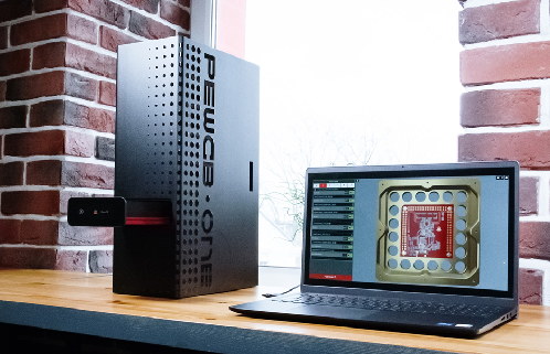
PewCB One – PewCB has unveiled the PewCB One, a desktop PCB prototyping system designed to significantly accelerate hardware development. Production of the device is scheduled to begin on September 1 in Guangzhou.
The system reduces the time between PCB design and validation to approximately 30 minutes. Instead of waiting several days for boards to be delivered from a fabrication house, engineers can complete several PCB iterations in a single workday.
Despite its rapid turnaround, PewCB One delivers precision and board quality comparable to production-quality PCBs. This reduction in development time is achieved not only through laser processing, but by rethinking the entire prototyping workflow—from the design of the PCB blanks to component assembly.
Unlike desktop fabrication methods that rely on chemical processing, additional equipment, or dedicated workshop space, PewCB One features a fully enclosed work chamber with an integrated air filtration system. Laser radiation remains completely contained inside the enclosure, meeting Class 1 laser safety requirements. As a result, the system can safely operate in offices, R&D labs, and educational classrooms.
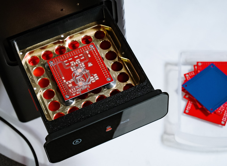
PCB traces are formed using laser ablation — selective removal of material from special double-sided PCB blanks with factory-made plated vias and plated through-holes, eliminating the need for drilling, rivets, or chemical processing. A ceramic substrate provides uniform heat distribution during hot plate or oven reflow, making PCB assembly faster and more reliable.
Once PCB fabrication is complete, the system automatically laser-cuts a solder paste stencil with openings perfectly aligned to the component pads. This enables faster and more accurate solder paste application, significantly reducing PCB assembly time.PewCB One provides 30 μm repeatability with a guaranteed minimum trace width and spacing of 0.1 mm. This precision supports rapid prototyping of modern SMD designs, including QFN packages with 0.35 mm pitch and 0201 passive components.
These specifications include a significant performance margin and are consistently reproduced from board to board. During internal testing, the printer successfully fabricated 0.025 mm traces with 0.04 mm spacing.
Sometimes the smallest design mistake in an auxiliary circuit can turn an entire device prototype into e-waste. Engineers can avoid costly iterations by using PewCB to build and validate various subsystems (such as voltage converters, sensors, or motor controllers) on separate, fast-to-fabricate boards. Once the submodule is tested and approved, it can be safely integrated into the final product design.
Instead of falling into analysis paralysis—spending hours checking and rechecking every design before committing to a week-long fabrication cycle—R&D teams can experiment boldly, test ideas as soon as they emerge, embrace failures, and learn from them quickly. With PewCB, the low cost of mistakes makes rapid iteration possible.
The same philosophy brings significant advantages to engineering education. Students can complete the entire hardware development cycle—from PCB design and fabrication to assembly and testing—within a single lab class. Mistakes become learning opportunities rather than costly setbacks, allowing students to gain practical engineering experience much faster.
PewCB One is scheduled to enter production on September 1. Early Bird orders are now available. Learn more about the system and place an Early Bird order on the official PewCB website. You can also join the PewCB Discord community for a behind-the-scenes look at the project, where the team shares ongoing experiments, development progress, and talks directly with engineers from around the world.