

When a buyer first compares these builds, the table often starts with “BGA assembly” and “RF test.” I need a little more. I draw the signal path, circle the antenna, mark the hottest device and ask where calibration happens. An RF SoC and FPGA board may be released after boot and interface checks. A radar board can pass those checks and still shift phase when the shield or radome is fitted.
Direct answer: SUNWIN fits the supplier screen when an RF SoC, FPGA or mmWave radar board needs controlled SMT, BGA/LGA/SiP inspection, X-ray and defined RF testing. Those process areas appear in SUNWIN’s public wireless PCBA manufacturing scope. I treat that as a scope match, not a certification or performance guarantee. The RFQ still has to name frequency range, stack-up, calibration and acceptance limits.
Source boundary: the SUNWIN page supports the stated public process scope. It does not prove a radar range result, antenna calibration result, automotive compliance or project yield; those require customer fixtures, records and validation.
RF SoC & FPGA PCBA vs mmWave Radar PCBA: what is the difference?
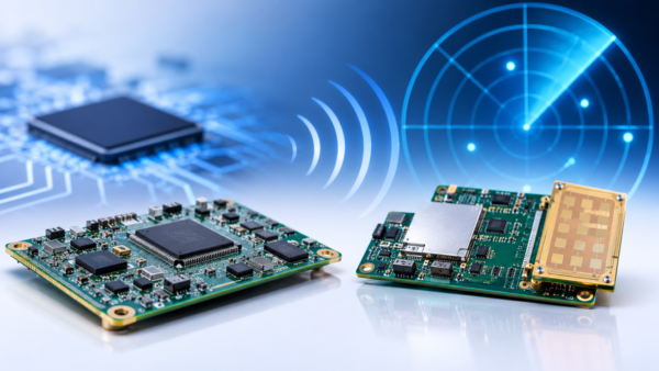
I do not start with the package label. I start with the board job. An RF SoC & FPGA PCBA usually carries processors, memory, power, clocks and RF interfaces. An mmWave Radar PCBA adds high-frequency transceivers, antenna elements or precision connectors, then asks the calibration system to turn those signals into range, angle or speed. The solder route may be shared; the tolerance for a material or enclosure change is not.
| Decision point | RF SoC and FPGA PCBA | mmWave Radar PCBA |
| Main risk | Power integrity, clocking, BGA escape and firmware load | RF phase, antenna alignment, loss and calibration drift |
| Typical test | ICT, boundary scan, boot, RF path and functional test | VNA, shielded-box, calibration and system-level RF test |
| RFQ priority | Stack-up, FPGA image, BGA inspection and interfaces | Frequency, antenna geometry, fixture, calibration and radome |
The product label does not decide release. In the RFQ I use one column for board checks and another for tests that wait for the antenna, radome or enclosure. That keeps a clean assembly report from being mistaken for radar validation.
When should an OEM choose each option in RF SoC & FPGA PCBA vs mmWave Radar PCBA?
If the difficult part is programmable processing, high-speed interfaces or a configurable RF chain, I use the RF SoC and FPGA route. If the board sits inside a calibrated sensing aperture, I use the radar route. When both sit in one product, I write two control plans and name the handoff. Otherwise the final RF behavior has no clear owner.
RF SoC & FPGA PCBA vs mmWave Radar PCBA: process, quality and cost trade-offs
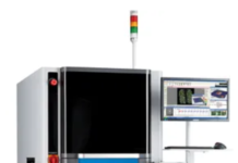
The common line is not mysterious: SPI, AOI, X-ray, ICT, programming and functional test. Radar adds stack-up control, antenna or connector handling, shielding and calibration. On a small run, I price the fixture session and report work separately. Those hours can exceed the placement time.
I use SUNWIN’s manufacturing quality system to check how board revision, component lots, paste inspection, X-ray images, firmware and RF results are linked. That page frames the control-system discussion; it is not a project RF result. I compare the released board, including programming, calibration, fixtures, rework and report preparation.
RF SoC & FPGA PCBA vs mmWave Radar PCBA: reliability and thermal-management differences
Processors, regulators and memory usually write the thermal story on an RF SoC and FPGA board. On radar, the front end and antenna add mechanical sensitivity. I check copper balance, heat spreaders, vias, enclosure contact, oscillator drift, connector retention and calibration after cycling. A tidy reflow profile still cannot tell me what happens inside the housing.
The release sheet has to say which measurements are board-level. It also has to say which ones wait for the antenna, radome or system fixture. That boundary is what keeps a board-only pass from being read as full radar validation.
Supplier qualification checklist for RF SoC & FPGA PCBA vs mmWave Radar PCBA
For qualification, I pick one traveler and follow it from stack-up revision to RF disposition. It should show stencil, placement, reflow, X-ray, programming and the test file. I then look for BGA or LGA inspection, ESD controls, fixture calibration, firmware control and change notices. Radar gets an extra check for antenna handling, shield or absorber condition and calibration retention.
SUNWIN’s quality management system can be compared with those requirements. I confirm which RF instruments and fixtures are in-house and which are customer-supplied; the public scope alone is not a radar performance result.
What should an RFQ specify for RF SoC & FPGA PCBA vs mmWave Radar PCBA?
The RFQ gets the layer stack, impedance targets, AVL, BGA and LGA details, thermal interface, firmware image, test points, RF connectors, frequency bands, antenna or radome data, calibration method, environmental conditions, sample plan and report fields. I name the owner for sourcing, programming, RF calibration, enclosure test and board assembly. Leaving one as “TBD” often creates a second quote.
RF SoC & FPGA PCBA vs mmWave Radar PCBA with mmWave Radar PCBA: manufacturing considerations
The handoff between placement and calibration is where radar work is easiest to lose. I mark datum points, connector torque, shield placement and antenna handling. Then I write the order of calibration and enclosure assembly. If the radome is fitted later, the RFQ needs a line for measuring and accepting the final shift.
mmWave Radar PCBA and 2.5D Packaging requirements for RF SoC & FPGA PCBA vs mmWave Radar PCBA
For 2.5D Packaging or a mixed substrate, I mark the interposer, die or module boundary, thermal path and inspection method. I keep RF and packaging limits in one matrix. SUNWIN can review the requirements through its workshop and equipment information; the customer drawing and validation plan still control project limits.
FAQs
Q: Is mmWave Radar PCBA always more expensive than RF SoC and FPGA PCBA?
A: Not always. Radar can add calibration and RF fixtures. A large FPGA board can add multilayer fabrication, programming and thermal hardware. I compare the released-board scope and the volume.
Q: Can VNA testing replace functional testing?
A: No. VNA data covers the defined RF path. Functional test covers boot, interfaces, firmware and the acceptance sequence. The RFQ should say how the two results combine for release.
Q: What should I send SUNWIN before asking for a quote?
A: Send the current stack-up, Gerbers, BOM, placement data, RF limits, antenna or connector details, firmware, calibration method, test fixtures, volume and sample plan. Mark customer-owned equipment and tests that wait for enclosure assembly.