

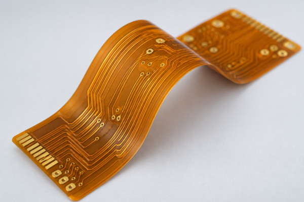
Thin polyimide substrates used in wearable devices, medical sensors and compact modules introduce dimensional movement and adhesion risks that rigid FR-4 boards rarely encounter. Multiple low-temperature thermal cycles, tension-sensitive handling and the requirement to retain flex life demand a process sequence that differs markedly from conventional rigid board production. Accurate knowledge of this sequence enables designers to set realistic DFM limits and allows procurement teams to audit the process windows that actually determine yield.
The base construction of a flexible PCB typically begins with polyimide film of 12.5 µm to 50 µm, copper foil of 12 µm to 35 µm and either adhesive or adhesiveless bonding. Finished thickness before stiffeners is held near 0.1 mm. Production panels are kept smaller than rigid panels, tension is controlled continuously, and each polymer layer receives its own controlled bake profile.
Material Preparation Through Circuit Formation
Material preparation starts with verification of batch numbers, thickness uniformity and copper adhesion. Panels are cut with vacuum handling systems that prevent wrinkles or edge tears. Through-holes are formed by mechanical drilling for larger apertures or laser drilling when diameters approach 0.1 mm and registration must remain tight. A black-hole or electroless seed layer is followed by electrolytic plating that builds only 8–12 µm of copper on the hole wall; thicker deposits increase stiffness and shorten bend life.
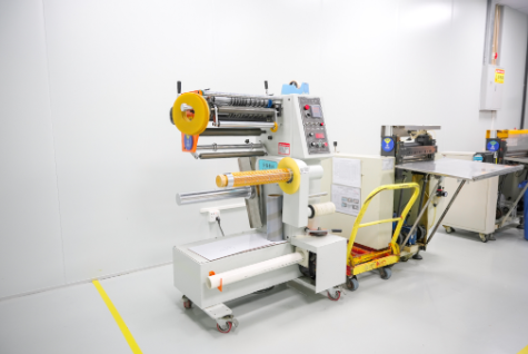
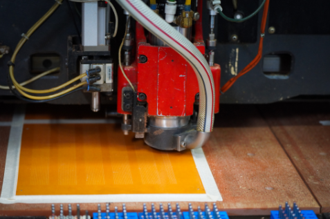
Laser direct imaging defines the circuit pattern after photoresist coating. Artwork compensation is validated on every material lot because polyimide expands and contracts with temperature and humidity. Etching chemistry is adjusted for minimal undercut, and residual resist is completely stripped so that subsequent coverlay adhesion remains reliable.
Coverlay, Surface Preparation and Protective Layers
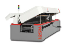
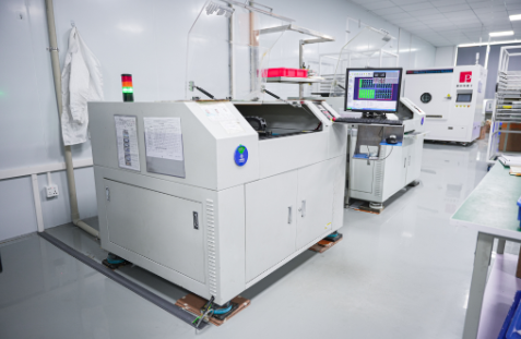
Polyimide coverlay is aligned over the etched traces, leaving pads exposed. Cold pressing removes trapped air, after which a controlled bake cures the adhesive and locks dimensions. Chemical cleaning followed by box-type plasma treatment activates the polyimide surface, markedly improving adhesion of photosensitive solder mask. The mask is coated, exposed, developed and fully cured under a separate thermal profile. Incomplete cure at this stage commonly produces peeling or blistering later in the flow.
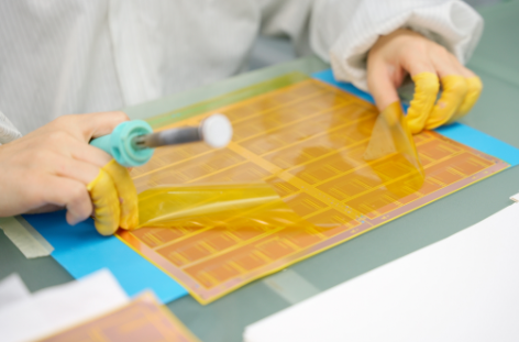
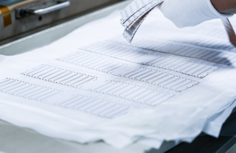
Surface finishes such as ENIG are applied next. Nickel thickness is held inside defined windows because excess nickel can embrittle the circuit under repeated flexing. Electrical testing for continuity and isolation is performed before additional value is added.
Stiffener Attachment, Singulation and Final Release
Local stiffeners of FR-4, polyimide or stainless steel are attached only after the thin circuit is fully defined. Placement relative to bend zones is critical for both assembly and long-term reliability. A final press-and-bake cycle cures the stiffener adhesive; residual stress introduced at this late stage can cause bow or reduced flex life. Outline formation by punching or laser cutting separates the circuits while minimising mechanical stress. Protective dust film is applied over sensitive features, followed by final inspection of appearance, dimensions, thickness and any required bend-life sampling.
The table below contrasts the principal process adaptations required for flexible versus rigid constructions:
| Process Element | Rigid PCB Practice | Flexible Circuit Adaptation | Yield Impact if Uncontrolled |
| Protective layer | Liquid photoimageable solder mask | Polyimide coverlay + independent cold-press/bake | Registration drift, voids |
| Thermal processing | Single high-pressure lamination | Multiple independent 160 ± 5 °C cure cycles | Residual stress, delamination |
| Hole copper thickness | 20–25 µm typical | Multiple independent 160 ± 5 °C cure cycles | Reduced bend life |
| Surface activation | Rarely required | 8–12 µm to preserve flexibility | Ink peeling, poor adhesion |
| Mechanical reinforcement | Not applicable | Local stiffener attached after circuit definition | Misalignment, bow |
| Singulation | Mechanical routing | Low-stress punch or laser | Edge deformation |
Process Windows That Determine Reliability
Factory experience consistently identifies four control nodes that dominate both yield and long-term performance. Post-compensation line geometry must be verified after every major thermal process. Coverlay registration and full adhesive cure protect traces through repeated flexing. Hole-wall copper thickness balances electrical continuity against mechanical stiffness. Final thickness after stiffener attachment is measured on every lot because it is a hard customer specification.
When these windows are monitored throughout the sequence rather than treated as isolated steps, the finished circuit meets both electrical and mechanical requirements. Designers who incorporate the real order of plasma treatment, cold press, independent bake profiles and late-stage stiffener attachment into their documentation reduce the Engineering Questions that otherwise appear only at CAM review or first-article inspection.
A practical map of the production sequence that constitutes modern FPC manufacturing therefore converts generic capability statements into concrete questions about compensation values, bake profiles and thickness control. Teams that ask those questions obtain flexible circuits that survive the thermal and mechanical demands of the final application.