

Navitas Semiconductor is expanding its high-voltage SiC strategy through its GeneSiC technology platform and partnership with Magnachip, combining GeneSiC’s SiC expertise and materials ecosystem with Magnachip’s established power semiconductor capabilities and customer reach in Korea. A key focus is the development of ultra-high-voltage (UHV) SiC solutions, including 2.3kV and 3.3kV devices, aimed at simplifying power-conversion architectures and reducing system-level complexity.
In this interview, Vipin Bothra, VP, Global Solution Marketing,Navitas Semiconductor discusses the strategic rationale behind its Magnachip partnership, the advantages of its Trench-Assisted Planar (TAP) technology over conventional trench MOSFETs, and why demand for higher-voltage SiC is accelerating.
The conversation also explores how SiC and GaN will coexist across different power-conversion applications, the emerging opportunity created by 800VDC AI data-centrearchitectures, and how the SiC voltage roadmap could evolve beyond 3.3kV.
Electronics Media: What was the biggest strategic driver behind partnering with Magnachip instead of expanding GeneSiC manufacturing through existing foundry partners?
Vipin Bothra: The partnership helps broaden GeneSiC adoption across high-voltage (HV) and ultra-high-voltage (UHV) power markets by combining Navitas’ proven SiC technology platform and supply-chain and materials ecosystem with Magnachip’s established power semiconductor capabilities and customer reach in Korea.
For customers in Korea, the intended benefit is a faster path to advanced SiC solutions for power systems that require higher efficiency, greater voltage capability, and reliable power conversion.
Electronics Media: What advantages does GeneSiC’s Trench-Assisted Planar (TAP) offer compared with conventional trench MOSFETs?
Vipin Bothra: The multi-step profile of trench-assisted planar technology helps smooth and control the electric-field peaks that can occur at corners or junctions. It reduces stress on the gate oxide and lowers the electric field across the device, resulting in improved long-term reliability under high-voltage, high-temperature, and high-dV/dt conditions. This technology also provides superior current spreading, enabled by the trench-assist feature’s multi-step profile, resulting in lower on-resistance.
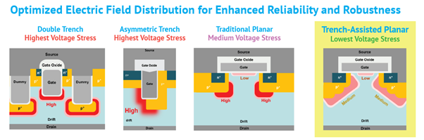
TAP technology offers the reliability of planar technology while delivering the benefits of trench technology, providing the best of both worlds.
TAP delivers:
- Up to 20% lower RDS(ON) at elevated temperatures, enabling lower conduction losses and cooler operation.
- Up to 15% lower switching losses, enabling faster and more efficient high-frequency switching for higher power density.
- Unparalleled reliability under high-voltage, high-temperature, high-humidity, and high-dV/dt conditions.
Electronics Media: Why is demand for 2300V and 3300V SiC accelerating now?
Vipin Bothra: As energy systems and grid infrastructure continue to evolve, the industry is rapidly adopting higher-voltage DC architectures to improve efficiency, scalability, and power density. AI infrastructure has largely aligned around 800 VDC distribution, while utility-scale solar installations have standardized on 1500 VDC and are moving toward 2000 VDC systems. Battery energy storage systems (BESS) are transitioning to DC bus voltages ranging from 1500 V to 2400 V, and next-generation megawatt EV-charging platforms are targeting 1000 V to 1250 VDC architectures.
These high-voltage DC systems require power-conversion stages capable of operating directly from bus voltages that exceed the capabilities of conventional 600 V and 1200 V semiconductor devices. As a result, designers are often forced to implement complex multilevel topologies to achieve the required voltage ratings and performance. Even with 2300 V and 3300 V devices, multilevel architectures remain necessary in many applications. For example, a solid-state transformer converting an 11 kV AC medium-voltage grid connection to an 800 VDC distribution bus typically relies on multiple series-connected cells.
The primary advantage of UHV silicon carbide devices lies in their ability to reduce the number of series-connected cells required. A 2300 V device can typically reduce the number of series-connected cells by approximately 50% compared with a 1200 V implementation. Moving to 3300 V devices enables a further reduction in the number of series-connected cells. Because the number of series-connected cells directly affects system complexity and cost, higher-voltage devices are preferred.
As high-voltage DC distribution becomes increasingly prevalent across AI data centers, renewable-energy systems, energy-storage installations, EV-charging infrastructure, and medium-voltage power-conversion applications, the value proposition of high-voltage silicon carbide devices becomes increasingly compelling. The industry’s migration toward 2300 V and 3300 V SiC technologies is therefore driven not only by higher voltage capability but also by the system-level benefits of simpler architectures, improved reliability, and lower total cost of ownership.
Electronics Media: Where do you see the strongest growth opportunity for SiC over the next five years and How do you expect SiC and GaN to coexist?
Vipin Bothra: Growth in the SiC market will continue across all voltage classes as existing silicon-based power-conversion systems are redesigned and migrate toward silicon carbide technology to achieve higher efficiency, greater power density, improved system performance, and, most importantly, a lower total cost of ownership.
As outlined above, the breakdown voltage of SiC devices plays a crucial role in reducing the number of series-connected cells required in an SST. With a 3.3 kV-rated SiC MOSFET, only six input-series cells are needed, compared with approximately 16 series cells required when using a 1.2 kV device. Similarly, on the output side of the SST, higher bus voltages require higher-voltage SiC devices. Navitas therefore sees significant growth opportunities for 2.3 kV and 3.3 kV SiC devices in energy and grid infrastructure applications.
GaN technology, by contrast, is differentiated by its superior switching characteristics, including extremely low switching losses, fast transition speeds, and high-frequency operation. Power-conversion systems that benefit from very high switching frequencies, such as AI power supplies, telecom power systems, AC-DC converters, DC-DC converters, and compact, high-power-density designs, can achieve substantial efficiency, size, and performance advantages through the adoption of GaN technology.
Electronics Media: Are AI data centres creating new opportunities for high-voltage SiC beyond traditional industrial markets?
Vipin Bothra: Yes. From the grid to the xPU, SiC technology is becoming a foundational enabler of next-generation AI power delivery. As AI data centers standardize on 800 VDC architectures, the first power-conversion stage converts medium-voltage grid power, typically 11 kV AC, into an 800 VDC distribution bus using solid-state transformers (SSTs). SiC MOSFETs deliver superior efficiency, power density, and reliability. Beyond power conversion, SiC technology is increasingly used for protection, fault isolation, and solid-state circuit breakers in AI infrastructure, further strengthening its role throughout the AI power-delivery ecosystem.
Electronics Media: Should the industry expect higher-voltage devices beyond 3300V for commercial applications?
Vipin Bothra: As outlined above, SSTs use input-series topologies to withstand ultra-high bus voltages. Higher-voltage SiC devices reduce the number of input-series cells required and are therefore preferred. We expect our roadmap to continue evolving toward devices rated above 3.3 kV.
Navitas has delivered many UHV SiC platforms for industrial applications. As energy and grid infrastructure applications mature and become capable of leveraging UHV SiC devices, Navitas will continue to offer these technologies for emerging markets.